
Process method to fully salicide (FUSI) both N-poly and P-poly on a CMOS flow

a technology of cmos flow and process method, which is applied in the direction of semiconductor/solid-state device manufacturing, basic electric elements, electric apparatus, etc., can solve the problems of single work function metal, reduced benefits otherwise provided by thin gate dielectrics, and increased percentage, so as to facilitate the adjustment and balancing of work functions, the effect of facilitating the increase of packing density

Active Publication Date: 2011-06-14
TEXAS INSTR INC
View PDF9 Cites 0 Cited by
  • Summary
  • Abstract
  • Description
  • Claims
  • Application Information

AI Technical Summary

Benefits of technology

This approach ensures more evenly matched FUSI gate formation in both NMOS and PMOS regions, reducing the risk of gate oxide punch-through and enabling efficient CMOS fabrication with improved packing densities and performance.

Problems solved by technology

This increased percentage significantly reduces the benefits otherwise provided by thinner gate dielectrics.
An inherent limitation of such metal gates, however, led to the use of polysilicon gates.
In particular, the use of a single work function metal proved to be a limitation in high performance circuits that require dual work function electrodes for low power consumption.
A single metal can not be used, however, to produce a metal gate that provides such different work functions.
However, polysilicon gates suffer from the aforementioned gate depletion.
Thus, for CMOS technologies with FUSI gates, the different work functions required for each of the NMOS and PMOS portions of the CMOS device present a fabrication challenge as both types are usually required in the same device and may also require different dopant species in the doping process.
In addition, the silicide typically forms at different rates in the NMOS and PMOS devices to the point where it may be difficult to obtain a controllable or stable silicidation process.
Because of these differing formation rates and the instability of the conventional process, the gate silicide formation occurring in a PMOS transistor may be yet incomplete, while an NMOS type transistor in the same device may have excessively formed and punched through the gate oxide layer.

Method used


Image

  • Process method to fully salicide (FUSI) both N-poly and P-poly on a CMOS flow
  • Process method to fully salicide (FUSI) both N-poly and P-poly on a CMOS flow
  • Process method to fully salicide (FUSI) both N-poly and P-poly on a CMOS flow

Examples


Embodiment Construction

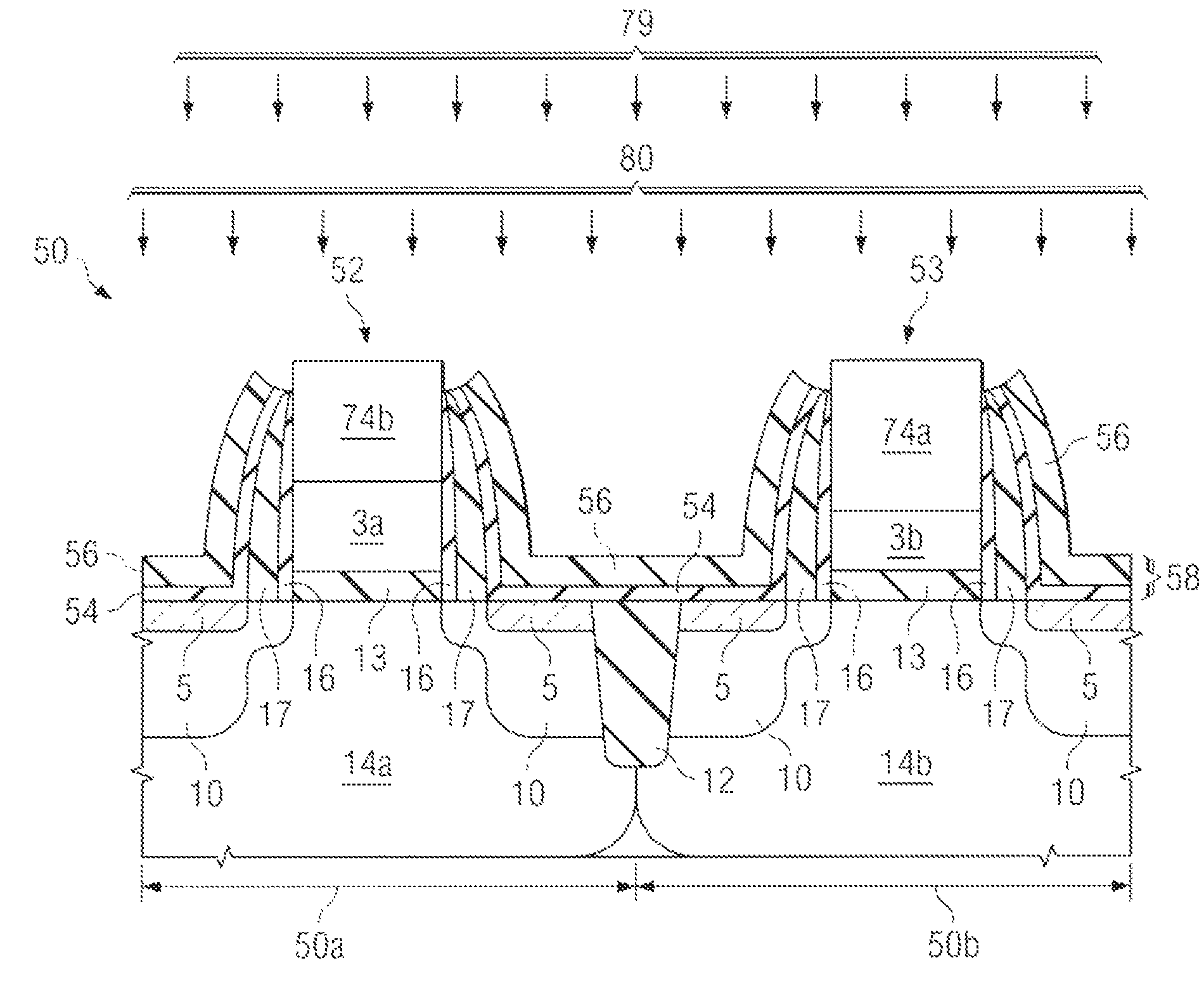
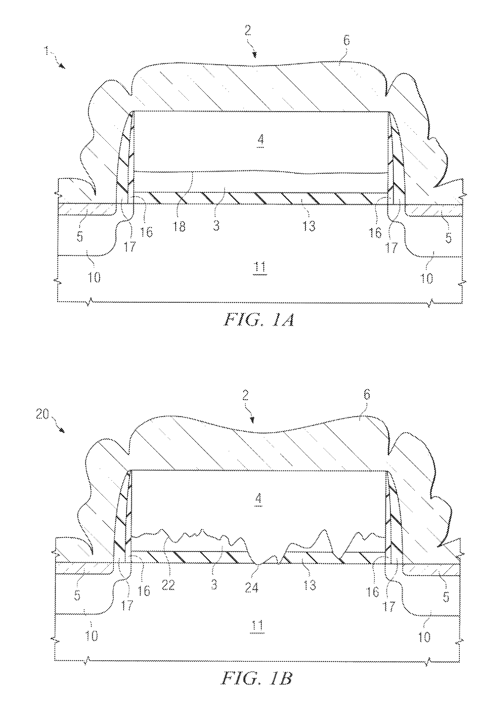
One or more aspects of the present invention are described with reference to the drawings, wherein like reference numerals are generally utilized to refer to like elements throughout, and wherein the various structures are not necessarily drawn to scale, it will be appreciated that where like acts, events, elements, layers, structures, etc. are reproduced; subsequent (redundant) discussions of the same may be omitted for the sake of brevity, in the following description, for purposes of explanation, numerous specific details are set forth in order to provide a thorough understanding of one or more aspects of the present invention. It may be evident, however, to one of ordinary skill in the art that one or more aspects of the present invention may be practiced with a lesser degree of these specific details. In other instances, known structures are shown in diagrammatic form in order to facilitate describing one or more aspects of the present invention.

Turning to FIGS. 1A and 1B, a pr...


PUM


Abstract

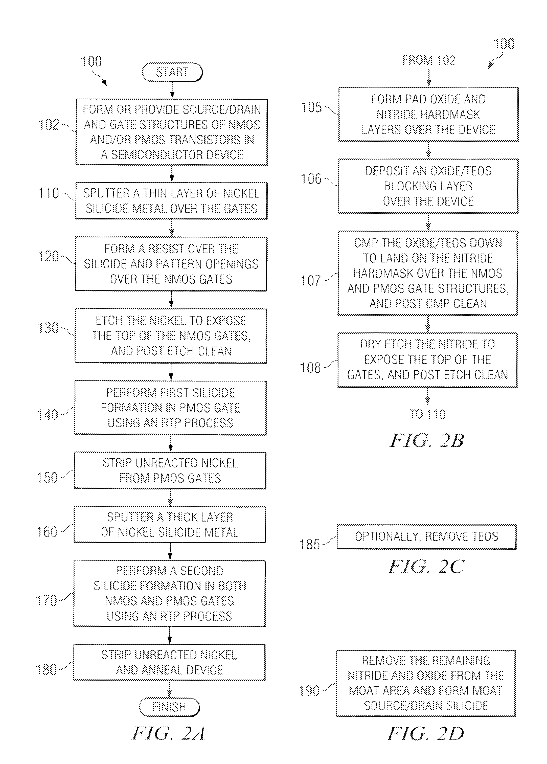
An improved method of forming a fully silicided (FUSI) gate in both NMOS and PMOS transistors of the same MOS device is disclosed. In one example, the method comprises forming a first silicide in at least a top portion of a gate electrode of the PMOS devices and not over the NMOS devices. The method further comprises concurrently forming a second silicide in at least a top portion of a gate electrode of both the NMOS and PMOS devices, and forming a FUSI gate silicide of the gate electrodes. In one embodiment, the thickness of the second silicide is greater than the first silicide by an amount which compensates for a difference in the rates of silicide formation between the NMOS and PMOS devices.

Description

FIELD OF INVENTIONThe present invention relates generally to semiconductor devices and more particularly to an innovative method of fabricating fully salicide (FUSI) poly gates of both PMOS and NMOS transistor devices of a CMOS process in a manner that provides a more evenly matched silicidation between the NMOS and PMOS transistor types of the same device.BACKGROUND OF THE INVENTIONIt can be appreciated that several trends presently exist in the electronics industry. Devices are continually getting smaller, faster and requiring less power, while simultaneously being able to support and perform a greater number of increasingly complex and sophisticated functions. One reason for these trends is an ever increasing demand for small, portable and multifunctional electronic devices such as cellular phones, personal computing devices, and personal sound systems are devices which are in great demand in the consumer market.Accordingly, there is a continuing trend in the semiconductor indust...

Claims


Application Information

Patent Timeline
Patent Type & Authority Patents(United States)
IPC IPC(8): H01L21/44
CPCH01L21/823835
Inventor MEHRAD, FREIDOONJOHNSON, FRANK S.
Owner TEXAS INSTR INC
Learn More