
Low-temperature formation of layers of polycrystalline semiconductor material

a polycrystalline semiconductor and low-temperature technology, applied in chemical vapor deposition coatings, electrical devices, coatings, etc., can solve the problems of time-consuming and consequently expensive methods described by do young kim et al., and achieve the effect of increasing the polycrystallinity of the semiconductor material and increasing the grain siz

Active Publication Date: 2011-06-21
INTERUNIVERSITAIR MICRO ELECTRONICS CENT (IMEC VZW)
View PDF1 Cites 6 Cited by
  • Summary
  • Abstract
  • Description
  • Claims
  • Application Information

AI Technical Summary

Benefits of technology

The present invention provides a method for forming a layer of polycrystalline semiconductor material on a substrate that is low temperature, simple, and compatible with low temperature processes. The method uses a catalyst particle that acts as an initiator, and a precursor gas that is plasma enhanced. The method can be performed at temperatures between room temperature and 500°C, and can be used with a variety of substrate materials such as semiconductor materials, glass, or plastic. The method is also suitable for doping the polycrystalline semiconductor material with dopant elements. The invention provides a method that is applicable to manufacturing processes of semiconductor devices and can be used in various industries.

Problems solved by technology

These methods require or a high-temperature (higher than 600° C.) deposition or thermal annealing for a long time.
The method described by Do young Kim et al. is time consuming and consequently also expensive.

Method used


Image

  • Low-temperature formation of layers of polycrystalline semiconductor material
  • Low-temperature formation of layers of polycrystalline semiconductor material
  • Low-temperature formation of layers of polycrystalline semiconductor material

Examples


example

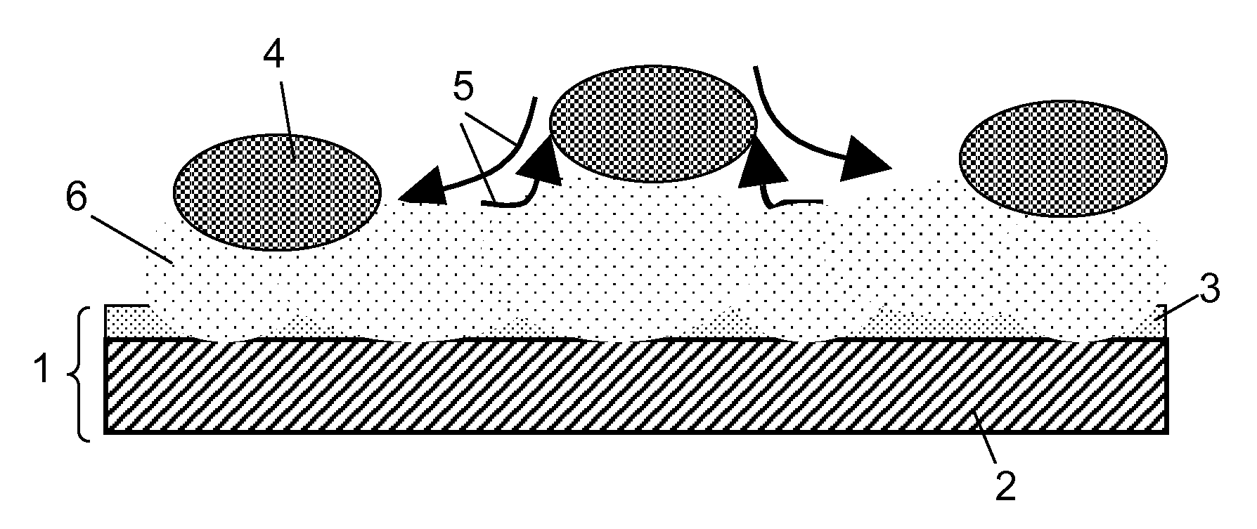
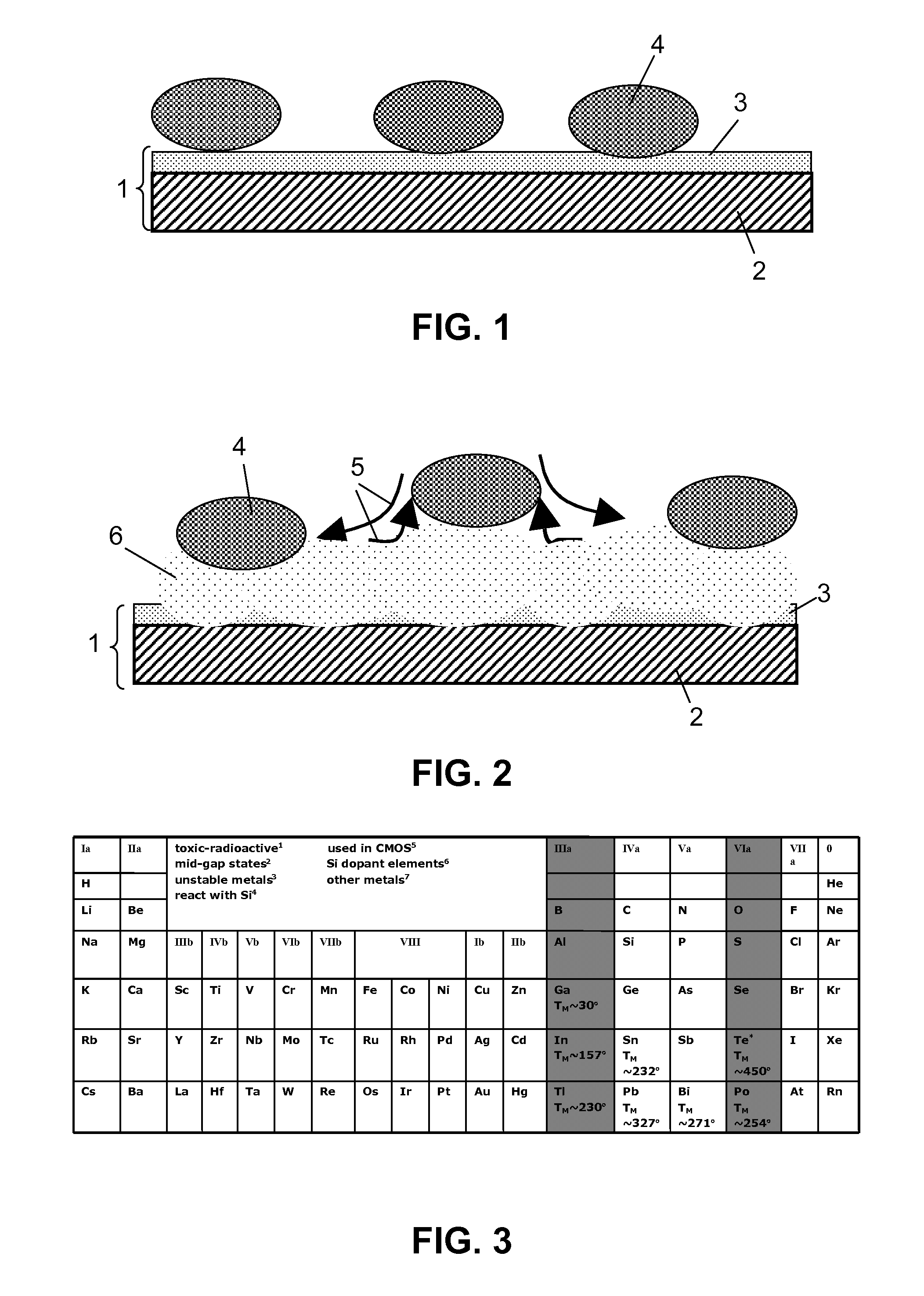
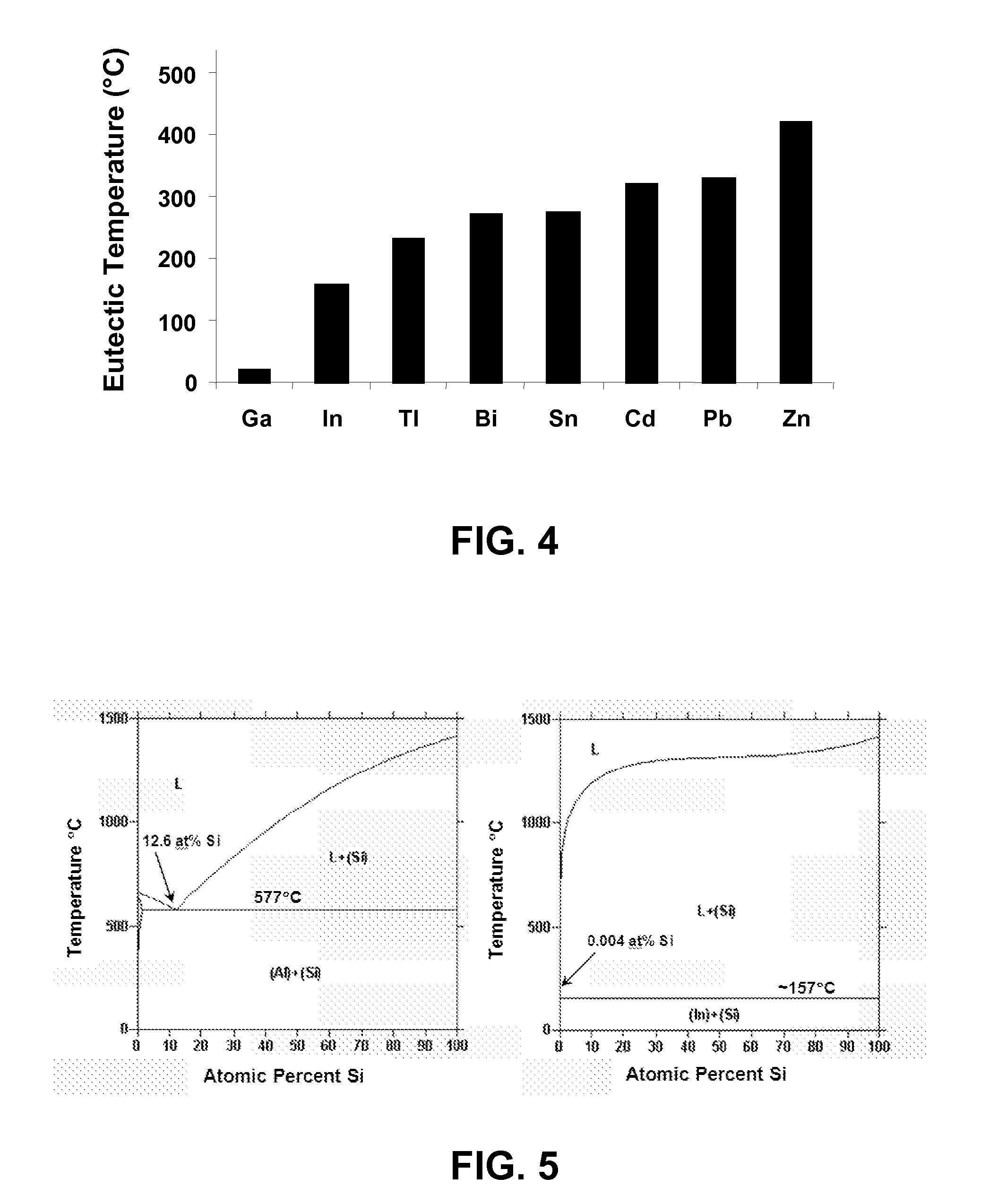
[0103]According to an example, Indium (In) may be used as a catalyst material. In has a melt temperature of 160° C. and is thus in liquid form at a temperature of 300° C. which is used in this experiment for forming the layer 6 of polycrystalline silicon.

[0104]The formation of a polycrystalline silicon layer was performed using VLS growth in a CVD chamber with a direct RF plasma source as described above by using the following recipe:[0105]1) Deposit catalyst particles 4 at a density in the order of 108 à 109 particles / cm2, the particles having a diameter of between 1 nm and 200 nm,[0106]2) heat up for 2 minutes, 300° C.,[0107]3) H2-preclean, 200 sccm, P=1000 mTorr, RF=100 W, 1 minute[0108]4) Pump down to 10 mTorr,[0109]5) Plasma deposition[0110]a. SiH4=20 sccm, H2=10 sccm, Ar=10 sccm (2:1:1)[0111]b. P=500 mtorr[0112]c. RF=20 W[0113]d. T=300° C.[0114]e. Time=10 min[0115]6) Pump down to 10 mTorr

[0116]For experiments, the following settings of the CVD chamber have been used: 200 mm wa...


PUM

PropertyMeasurementUnit
temperatureaaaaaaaaaa

Abstract

The present invention provides a method for forming a layer (6) of polycrystalline semiconductor material on a substrate (1). The method comprises providing at least one catalyst particle (4) on a substrate (1), the at least one catalyst particle (4) comprising at least a catalyst material, the catalyst material having a melt temperature of between room temperature and 500° C., or being able to form a catalyst material / semiconductor material alloy with a eutectic temperature of between room temperature and 500° C., and forming a layer (6) of polycrystalline semiconductor material on the substrate (1) at temperatures lower than 500° C. by using plasma enhancement of a precursor gas, thereby using the at least one catalyst particle (4) as an initiator. The present invention furthermore provides a layer (6) of polycrystalline semiconductor material obtained by the method according to embodiments of the present invention.

Description

CROSS-REFERENCE TO RELATED APPLICATIONS[0001]This application is the national phase under 35 U.S.C. §371 of PCT International Application No. PCT / EP2008 / 052018 which has an International filing date of Feb. 19, 2008, which designates the United States of America, and which claims the benefit of U.S. Provisional Application No. 60 / 890,573 filed Feb. 19, 2007, the disclosures of which are hereby expressly incorporated by reference herein in their entirety and are hereby expressly made a portion of this application.TECHNICAL FIELD OF THE INVENTION[0002]The present invention relates to polycrystalline semiconductor material. More particularly, the present invention relates to a method for forming a layer of polycrystalline semiconductor material on a substrate and to layers of polycrystalline semiconductor material thus obtained.BACKGROUND OF THE INVENTION[0003]Formation of polycrystalline semiconductor material has been extensively studied over the years.[0004]Conventional ways of maki...

Claims


Application Information

Patent Timeline
Patent Type & Authority Patents(United States)
IPC IPC(8): C23C16/24H01L31/20H01L21/36H01L21/20H01L31/036H01L29/00
CPCH01L21/0237H01L21/02532H01L21/02595H01L21/02653H01L21/02576H01L21/02579H01L21/02645H01L21/0262
Inventor IACOPI, FRANCESCAVEREECKEN, PHILIPPE M.
Owner INTERUNIVERSITAIR MICRO ELECTRONICS CENT (IMEC VZW)
Learn More