
SAR ADC

Active Publication Date: 2011-06-21
TEXAS INSTR INC
View PDF9 Cites 22 Cited by
  • Summary
  • Abstract
  • Description
  • Claims
  • Application Information

AI Technical Summary

Benefits of technology

[0008]In accordance with a preferred embodiment of the present invention, a high input voltage can be sampled on the first plurality of capacitors (i.e. on a capacitive array, which may be a capacitive digital to analog conversion stage of a SAR ADC) without having to divide the input voltage before performing the conversion. The first plurality of capacitors is coupled with one side to a common node through which charge is redistributed during conversion. The voltage on the common node must converge during the successive approximation procedure and should not exceed the comparator input range. In order to handle input voltage levels higher than the maximum input voltage range of the comparator, the first conversion step (or steps) is performed by another ADC, i.e. ADC stage 202. ADC stage 202 may be any kind of ADC and it may advantageously have a lower overall performance than the first ADC stage (i.e. it may have lower signal to noise ratio, resolution etc.). Therefore, the second analog to digital conversion step may need less chip area or calibration. The second analog digital conversion stage may advantageously be used for bit decisions relating to the floating capacitor(s) of the first ADC stage. The floating capacitor(s) in the first ADC stage is (are) coupled to reference signal levels (ground is also considered as a reference signal level) in accordance with the decisions made by ADC stage 202. The floating capacitor(s) and the first plurality of capacitors are dimensioned such that convergence of the successive approximation procedure is ensured when the floating capacitor(s) is (are) coupled to the respective reference level. Since the full electrical charge of the input voltage is sampled with the first ADC stage and since the entire sampled charge remains on the capacitors during conversion, there is no loss of SNR compared with ADC which divide the input voltage before conversion.
[0011]In accordance with a preferred embodiment of the present invention, it also provides the advantage of a small error and any error that does arise may be corrected with a simple error correction scheme. Furthermore, the capacitors of the first ADC stage constitute only a small load on the reference input since the MSB capacitors (i.e. advantageously the floating capacitors) switch only a small number of times between the negative reference and the positive reference and the switching may not cause significant spikes or glitches at the comparator input. Glitching of the comparator inputs in the present invention is also irrelevant, since the capacitors are only switching once. More complex switching schemes may cause glitches and the comparator input nodes to rise above the supply voltage rail and / or below ground, which could discharge the nodes and cause forward biasing of diodes in the circuit, therefore leading to the capacitors being discharged. Here, the comparator input is kept in the allowed voltage range. Still further, the design of the device according to the present invention is uncomplicated and also minimizes time constraints so that the converter does not lose speed.
[0013]In accordance with a preferred embodiment of the present invention, the control stage may be adapted to perform a dynamic error correction procedure. This provides a reliable error correction, which can be carried out for some bit decisions or after each bit decision. The error correction may be necessary to ensure convergence of the analog to digital conversion procedure in the first ADC stage since at least one of the MSB decisions is performed by ADC stage 202, which may have lower performance than the first ADC stage. However, the error correction scheme provides sufficient safety to ensure convergence, even with an additional low performance second ADC stage.
[0014]ADC stage 202 may be adapted to use successive approximation. Furthermore, ADC stage 202 may comprise a second plurality of capacitors. In an advantageous aspect of the invention, ADC stage 202 may be operable to divide the input voltage before it is converted. If only ADC stage 202 divides the input signal, there is no loss in performance with respect to the first ADC stage. If the first and ADC stage 202s are implemented in a similar manner with capacitive arrays, they may even share the same comparator. Therefore, a comparator may be provided having inputs coupled to the first plurality of capacitors and the second plurality of capacitors for making alternately bit decisions with respect to the first plurality of capacitors and the second plurality of capacitors.

Problems solved by technology

However, more than one of the capacitors could also be left floating.
However, as the charge is frozen, it can be used later during the conversion process, even though it did not contribute to the conversion process during the first step or during several of the first steps.

Method used


Image

  • SAR ADC
  • SAR ADC
  • SAR ADC

Examples


Embodiment Construction

[0023]Refer now to the drawings wherein depicted elements are, for the sake of clarity, not necessarily shown to scale and wherein like or similar elements are designated by the same reference numeral through the several views.

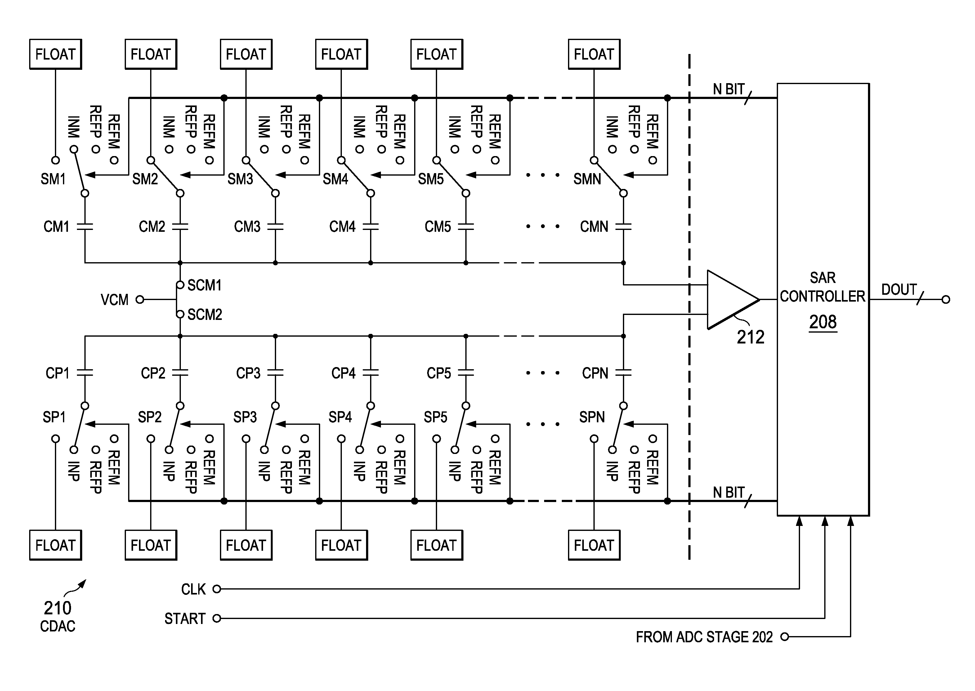
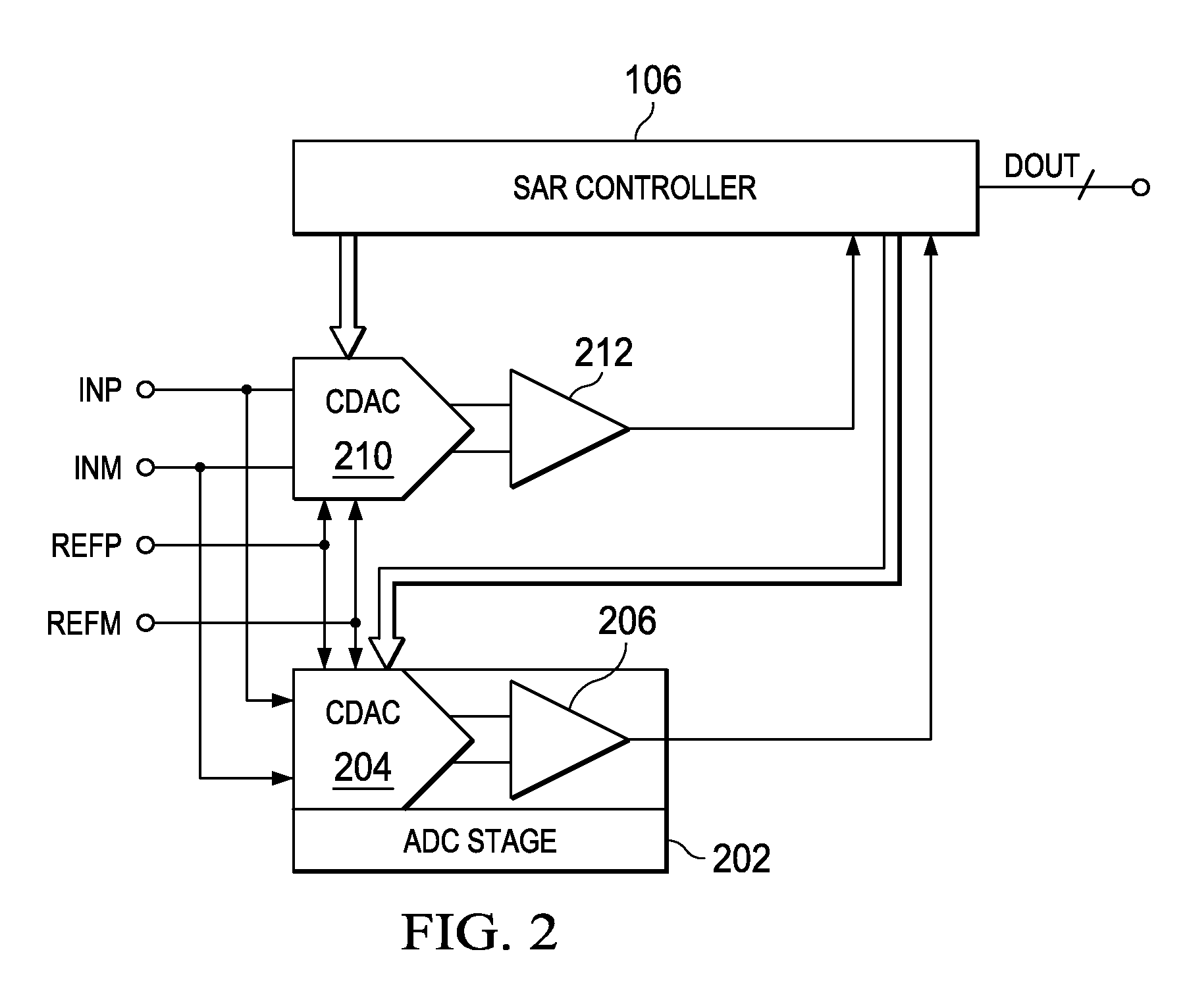
[0024]Referring to FIG. 2 of the drawings, the reference numeral 200 generally designates a successive approximation register (SAR) analog-to-digital converter (ADC) in accordance with a preferred embodiment of the present invention. A first ADC stage may include a switch capacitor array or capacitive digital-to-analog-converter (CDAC) 210 for evaluating bits of an analog-to-digital conversion. The array 210 may be coupled to comparator 212. Comparator 212 outputs a signal to a SAR controller 208, which may indicate the comparison result of comparator 212. ADC stage 202 can also be coupled to the SAR controller 208.

[0025]ADC stage 202 may be any kind of ADC stage. However, as shown, ADC stage 202 generally includes a CDAC or switched capacitor array 204 and co...


PUM


Abstract

An electronic device is provided for analog to digital conversion using successive approximation. The device comprises a first ADC stage. The first ADC stage includes a first plurality of capacitors adapted to sample an input voltage, and adapted to be coupled to either a first reference signal level or a second reference signal level. At least one capacitor of the first plurality of capacitors is adapted to be left floating. A control stage is adapted to switch the at least one floating capacitor to the first reference signal level or the second reference signal level in response to an analog to digital conversion decision made by a second ADC stage.

Description

CROSS REFERENCE TO RELATED APPLICATIONS[0001]This application is claims priority to German Patent Application No. 102008035215.2, filed on Jul. 29, 2008, and to U.S. Patent Application Ser. No. 61 / 141,425, filed on Dec. 30, 2008. Each application which is hereby incorporated by reference for all purposes.TECHNICAL FIELD[0002]The invention relates generally to an electronic device and, more particularly, to a successive approximation register (SAR) analog-to-digital converter (ADC).BACKGROUND[0003]Successive approximation is one of the techniques used for analog-to-digital conversion. The general functionality and operation of successive approximation register (SAR) analog-to-digital converters (ADCs) is well known in the art. SAR ADCs compare the analog input voltage to reference signal levels, which can be generated by a digital-to-analog converter (DAC). During a first clock cycle, the sampled input voltage may be compared to half the reference signal output by the DAC. If the res...

Claims


Application Information

Patent Timeline
IPC IPC(8): H03M1/12
CPCH03M1/08H03M1/0682H03M1/804H03M1/468H03M1/124
Inventor OHNHAEUSER, FRANKWICKMANN, ANDREAS
Owner TEXAS INSTR INC
Features
  • Generate Ideas
  • Intellectual Property
  • Life Sciences
  • Materials
  • Tech Scout
  • Unparalleled Data Quality
  • Higher Quality Content
  • 60% Fewer Hallucinations
Learn More