

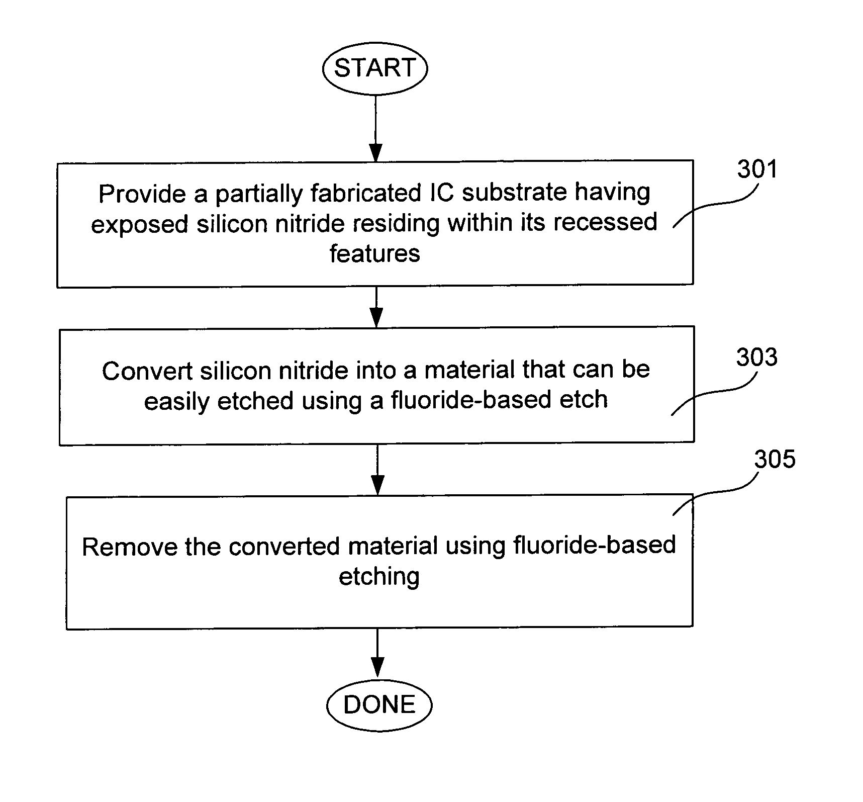
Methods for removing silicon nitride and other materials during fabrication of contacts
a technology of silicon nitride and other materials, applied in the direction of decorative arts, decorative surface effects, electric apparatus, etc., can solve the problems of large amounts of surrounding silicon oxide containing materials being inadvertently removed, material that may be difficult to remove, and damage to elemental silicon, etc., to achieve easy etching, easy etching with fluoride-based etches, and easy etching
- Summary
- Abstract
- Description
- Claims
- Application Information
AI Technical Summary
Benefits of technology
Problems solved by technology
Method used
Image

Examples
Embodiment Construction
Introduction and Overview
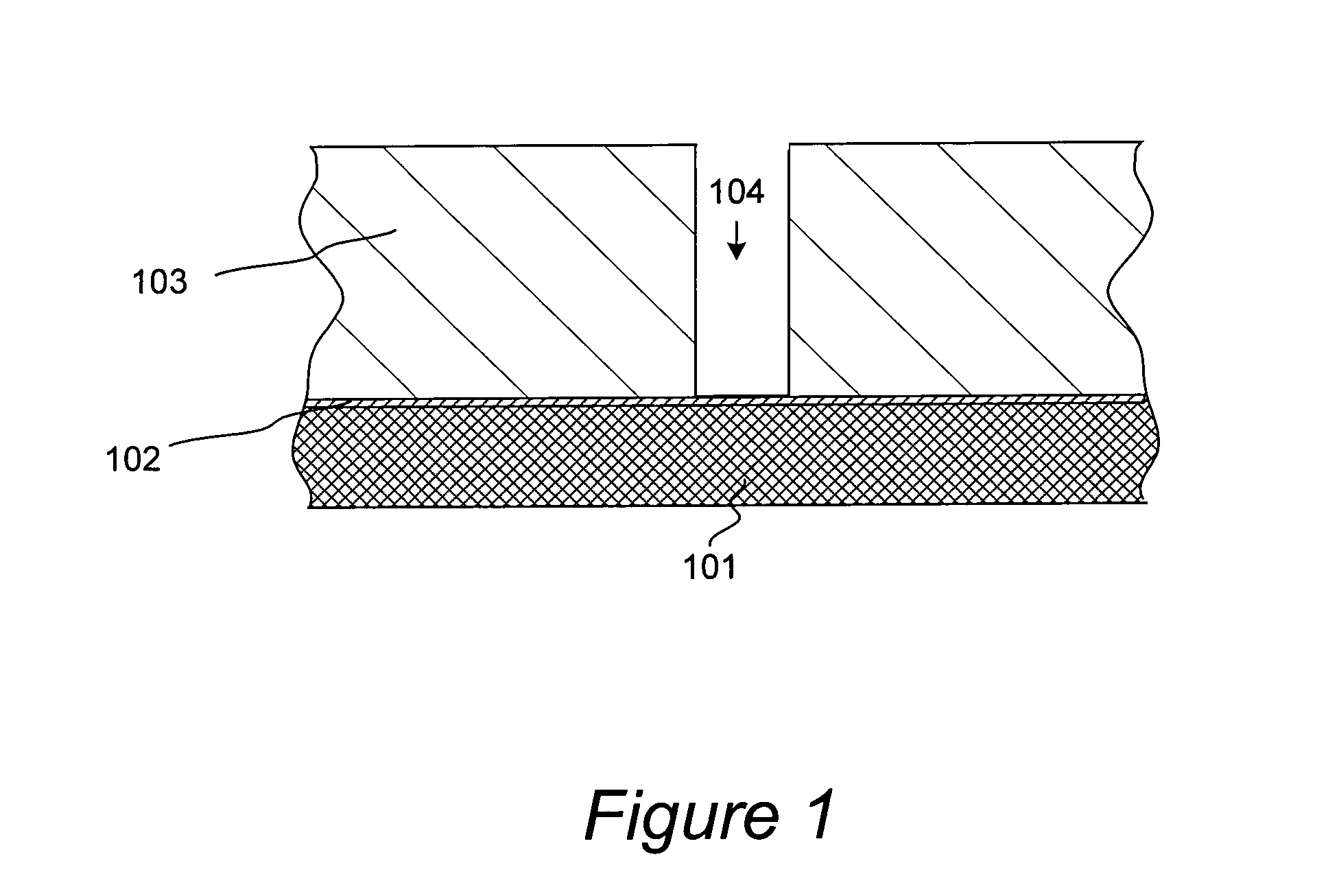
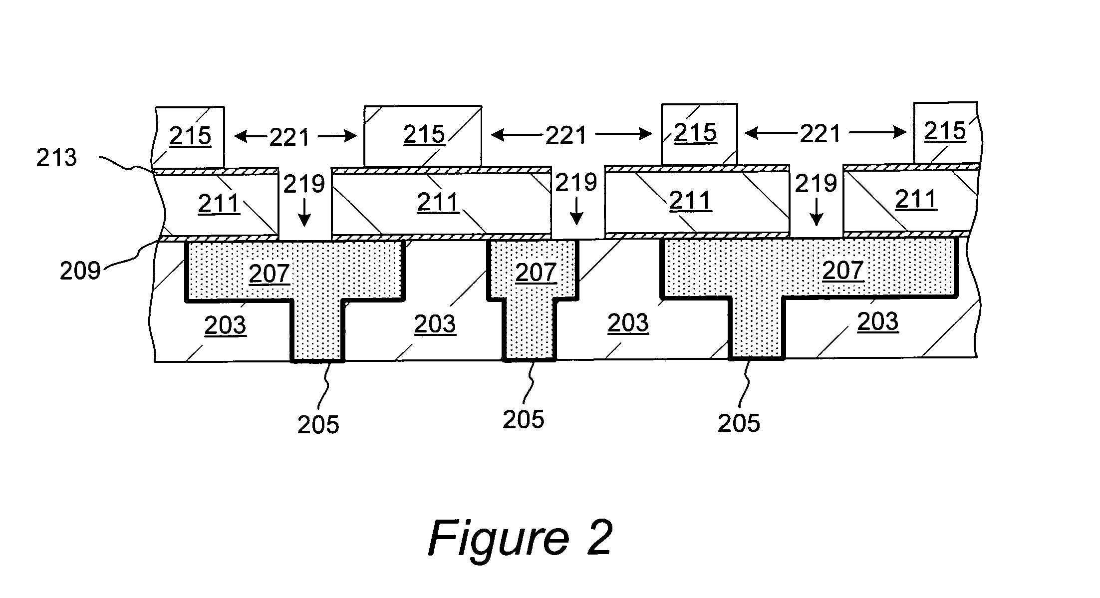
[0019]Removal of silicon nitride presents several challenges, which become more pronounced as the dimensions of recessed features in IC devices continue to shrink. Silicon nitride is often more resistant to fluoride-based etching than the surrounding silicon dioxide based ILD, and therefore often requires more aggressive etching conditions. Removal of even very small amounts of etch-resistant silicon nitride from the contacts and interconnects, can inadvertently result in etching of substantial amounts of silicon dioxide based ILD material, which defines the dimensions of recessed features on a partially fabricated IC device. While such inadvertent etching may be tolerated in some device structures with relatively large dimensions of recesses, in those structures where dimensions are small, fluoride-based etching of etch resistant silicon nitride may lead to substantial increase in critical dimensions of vias and trenches defining the contacts. Such increase...
PUM
| Property | Measurement | Unit |
|---|---|---|
| Critical dimension | aaaaa | aaaaa |
Abstract
Description
Claims
Application Information