Integrated circuit package system with dual connectivity

a technology of integrated circuits and integrated circuits, applied in the direction of electrical equipment, semiconductor devices, semiconductor/solid-state device details, etc., can solve the problems of inefficiency of kgd, difficult to test the die before assembly on the substrate, and the vertical or horizontal arrangement of multi-chip modules

Active Publication Date: 2011-07-12
STATS CHIPPAC LTD
View PDF25 Cites 7 Cited by
  • Summary
  • Abstract
  • Description
  • Claims
  • Application Information

AI Technical Summary

Problems solved by technology

However, multi-chip modules, whether vertically or horizontally arranged, can also present problems because they usually must be assembled before the component chips and chip connections can be tested.
That is, because the electrical bond pads on a die are so small, it is difficult to test die before assembly onto a substrate.
With conventional multi-chip modules, however, the die cannot be individually identified as KGD before final assembly, leading to KGD inefficiencies and assembly process yield problems.
But stacking integrated devices, package-in-package, package-on-package, or combinations thereof have assembly process difficulties caused by leaded packages having limited input and output (I / O) which limits its role 3D packaging.
Current leaded packages also do not provide the flexibility to support the various integration and stacking options described earlier with the higher I / O count support.
Solutions to these problems have been long sought but prior developments have not taught or suggested any solutions and, thus, solutions to these problems have long eluded those skilled in the art.

Method used


Image

  • Integrated circuit package system with dual connectivity
  • Integrated circuit package system with dual connectivity
  • Integrated circuit package system with dual connectivity

Examples


first embodiment

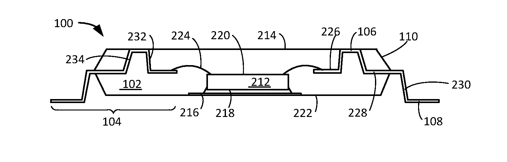
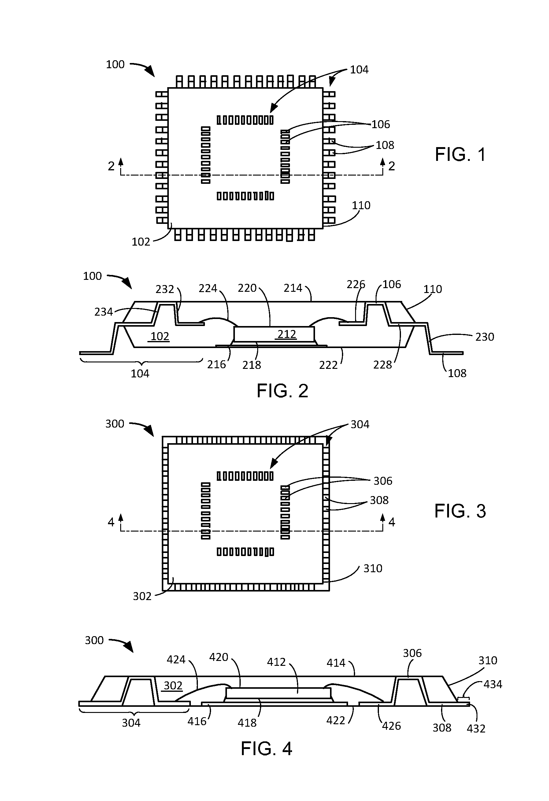
[0029]Referring now to FIG. 1, therein is shown a top view of an integrated circuit package system 100 in the present invention. The top view depicts a package encapsulation 102, such as an epoxy molding compound, and leads 104 exposed from the package encapsulation 102. The package encapsulation 102 exposes a top contact portion 106 of the leads 104 and the top contact portion 106 is placed away from the peripheral of the package encapsulation 102. A bottom contact portion 108 of the leads 104 extends from a nonhorizontal portion 110 of the package encapsulation 102. For example, the integrated circuit package system 100 is shown as a quad flat package (“QFP”) type.

[0030]For illustrative purposes, the integrated circuit package system 100 is shown with the top contact portion 106 and the bottom contact portion 108 of the leads 104 equally spaced. Although, it is understood that the integrated circuit package system 100 may have some sites depopulated such that the integrated circui...

second embodiment

[0034]Referring now to FIG. 3, therein is shown a top view of an integrated circuit package system 300 in the present invention. The top view depicts a package encapsulation 302, such as an epoxy molding compound, and leads 304 exposed from the package encapsulation 302. The package encapsulation 302 exposes a top contact portion 306 of the leads 304. The top contact portion 306 is placed away from the peripheral of the package encapsulation 302. A bottom contact portion 308 of the leads 304 extends from a nonhorizontal portion 310 of the package encapsulation 302. For example, the integrated circuit package system 300 is shown as a quad flat nonleaded (“QFN”) type package.

[0035]Referring now to FIG. 4, therein is shown a cross-sectional view of the integrated circuit package system 300 along line 4-4 of FIG. 3. The cross-sectional view depicts an integrated circuit die 412 and the leads 304 having the top contact portion 306 and the bottom contact portion 308 in the integrated circ...

third embodiment

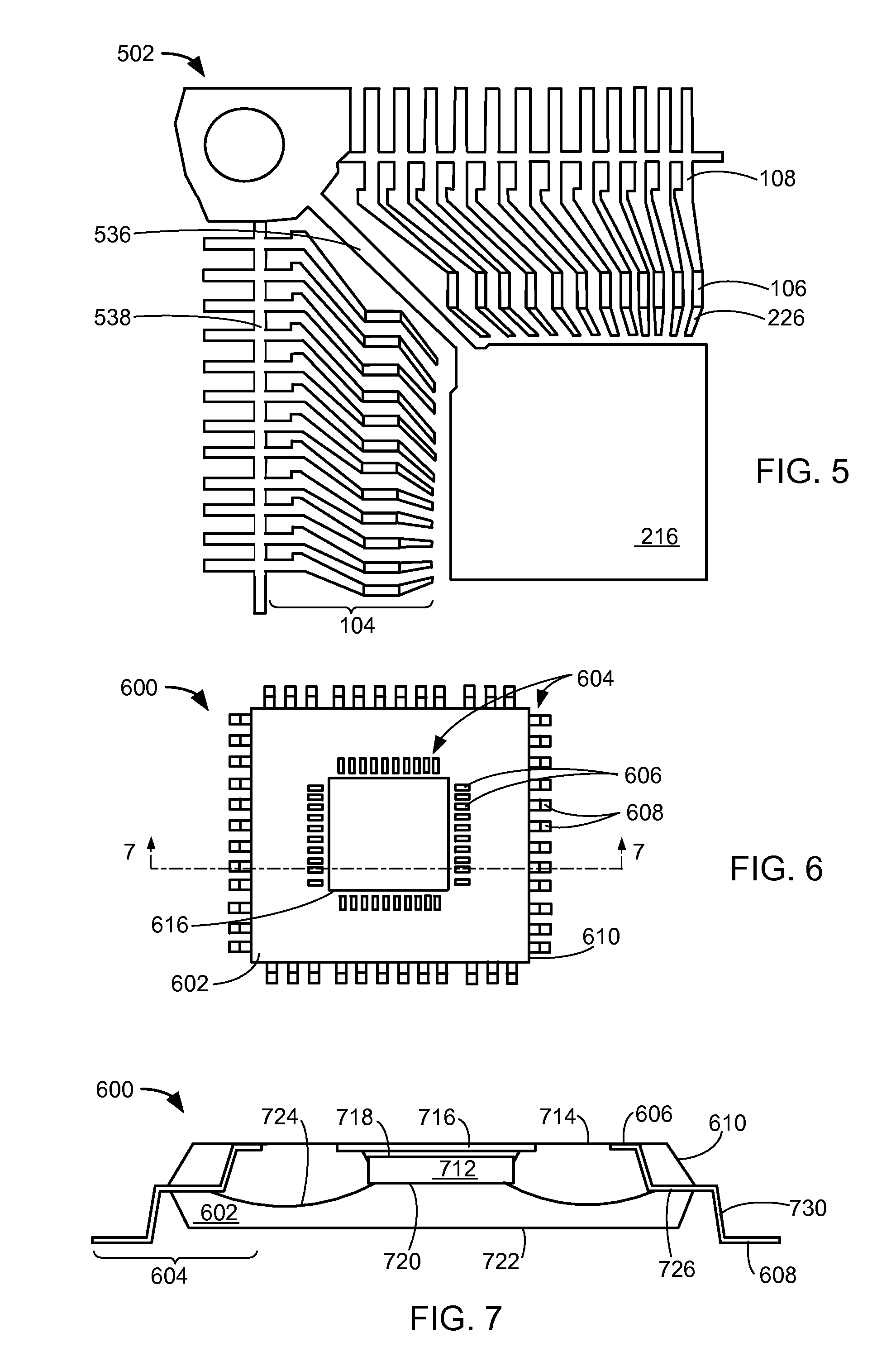
[0038]Referring now to FIG. 6, therein is shown a top view of an integrated circuit package system 600 in the present invention. The top view depicts a package encapsulation 602, such as an epoxy molding compound, and leads 604 exposed from the package encapsulation 602. The package encapsulation 602 exposes a top contact portion 606 of the leads 604. The top contact portion 606 is away from the peripheral of the package encapsulation 602. A bottom contact portion 608 of the leads 604 extends from a nonhorizontal portion 610 of the package encapsulation 602. The package encapsulation 602 exposes a die-attach paddle 616 surrounded by the top contact portion 606 of the leads 604. For example, the integrated circuit package system 600 is shown as a quad flat package (“QFP”) type.

[0039]Referring now to FIG. 7, therein is shown a cross-sectional view of the integrated circuit package system 600 along line 7-7 of FIG. 6. The cross-sectional view depicts an integrated circuit die 712 and t...


PUM


Abstract

An integrated circuit package system includes: forming a lead having a both top contact portion and a bottom contact portion; connecting an integrated circuit die and the lead; and forming a package encapsulation, having a top side and a bottom side, over the integrated circuit die. The forming the package encapsulation includes partially exposing the top contact portion at the top side, and partially exposing the bottom contact portion along the bottom side with the bottom contact portion extending beyond a nonhorizontal portion of the package encapsulation.

Description

TECHNICAL FIELD[0001]The present invention relates generally to an integrated circuit package system and more particularly to an integrated circuit package system with dual connectivity.BACKGROUND ART[0002]Increased miniaturization of components, greater packaging density of integrated circuits (“ICs”), higher performance, and lower cost are ongoing goals of the computer industry. Semiconductor package structures continue to advance toward miniaturization, to increase the density of the components that are packaged therein while decreasing the sizes of the products that are made therefrom. This is in response to continually increasing demands on information and communication products for ever-reduced sizes, thicknesses, and costs, along with ever-increasing performance.[0003]These increasing requirements for miniaturization are particularly noteworthy, for example, in portable information and communication devices such as cellular phones, hands-free cellular phone headsets, personal...

Claims


Application Information

Patent Timeline
Patent Type & Authority Patents(United States)
IPC IPC(8): H01L23/52H01L23/48
CPCH01L23/49551H01L23/552H01L25/105H01L2224/48091H01L2224/48247H01L2224/73265H01L2924/1532H01L2924/3025H01L2924/00014H01L24/48H01L2224/32245H01L2924/00H01L2225/1029H01L2225/1041H01L2225/1058H01L2224/45014H01L2924/14H01L2924/181H01L2924/00012H01L2224/45015H01L2924/207H01L2924/206
Inventor CAMACHO, ZIGMUND RAMIREZPISIGAN, JAIRUS LEGASPICAPARAS, JOSE ALVINTAY, LIONEL CHIEN HUI
Owner STATS CHIPPAC LTD
Why Eureka
Try Eureka