
Operational amplifier

a technology of operation amplifier and amplifier, which is applied in the direction of dc-amplifiers with dc-coupled stages, amplifiers with semiconductor devices/discharge tubes, and differential amplifiers. it can solve the problems of increasing power consumption, power consumption in each of the added circuits, and increasing power consumption. it reduces power consumption during idle state and improves slew ra

Inactive Publication Date: 2011-07-19
ABLIC INC
View PDF11 Cites 6 Cited by
  • Summary
  • Abstract
  • Description
  • Claims
  • Application Information

AI Technical Summary

Benefits of technology

This configuration reduces total power consumption and enables efficient operation with high supply voltages, enhancing the slew rate and reducing idle state current consumption without additional circuits, thus addressing the limitations of conventional methods.

Problems solved by technology

In this case, however, the increase of the power consumption comes up as a problem.
However, because those detection and control circuits are provided in parallel to the signal amplification circuit and the output driving circuit, the power consumption is made in those added circuits.
If the supply voltage is high, for example, if it is 5V or over, however, the power consumption in each of the added circuits provided in parallel to the amplifier increase proportionally to the supply voltage, so the idle state power consumption in added circuits limits the number of amplifiers integrated in one IC because of heat generated by idle current.
This has also been a problem and the present inventor et al. have found such conventional problems by themselves.

Method used


Image

  • Operational amplifier
  • Operational amplifier
  • Operational amplifier

Examples


first embodiment

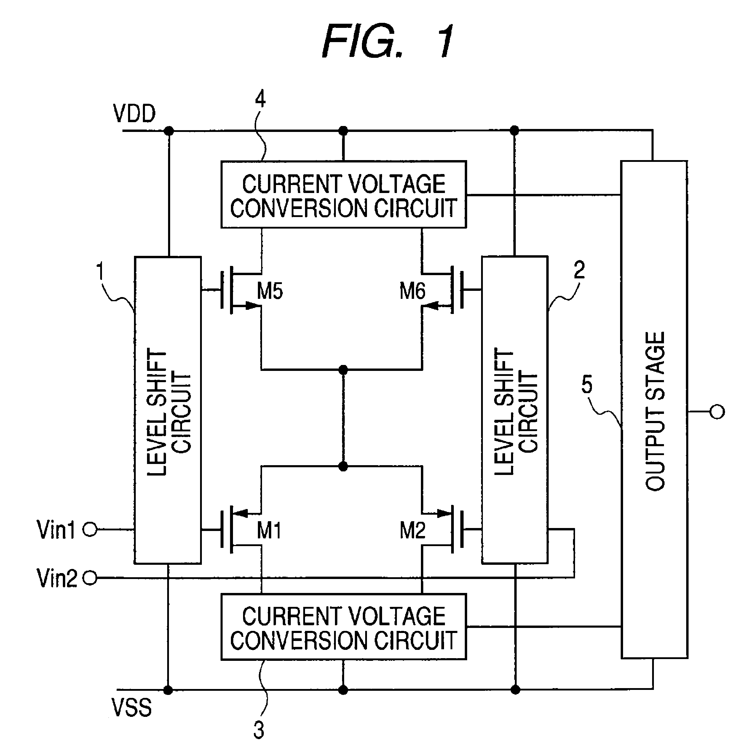
[0023]FIG. 1 is a block diagram of an operational amplifier for describing the basic principle of the present invention. Input signals Vin1 and Vin2 are inputted to level shift circuits 1 and 2 respectively. Each of the level shift circuits 1 and 2 has two outputs to output two converted signals to a PMOS differential pair and an NMOS differential pair respectively. The PMOS transistors M1 and M2 are paired to form a differential transistor pair while the NMOS transistors MS and M6 are paired to form a differential transistor pair. The drains of the PMOS transistors M1 and M2 are connected to a current voltage conversion circuit 3 and the drains of the NMOS transistors MS and M6 are connected to a current voltage conversion circuit 4. Each of the current voltage conversion circuits 3 and 4 converts an output current of a differential transistor pair to a voltage used for driving an output stage 5.

[0024]In case of a general operational amplifier, a differential transistor pair is bia...

second embodiment

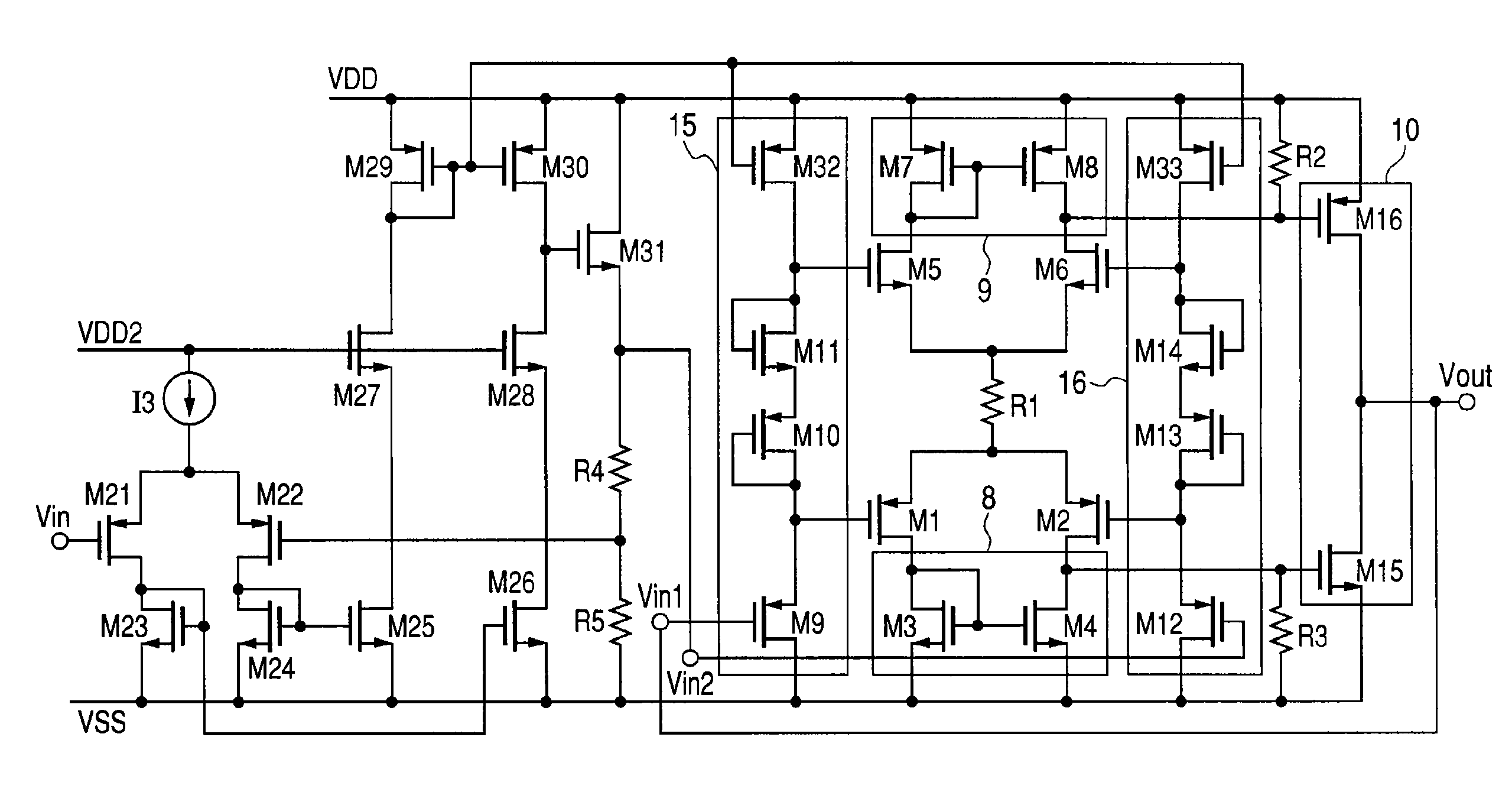
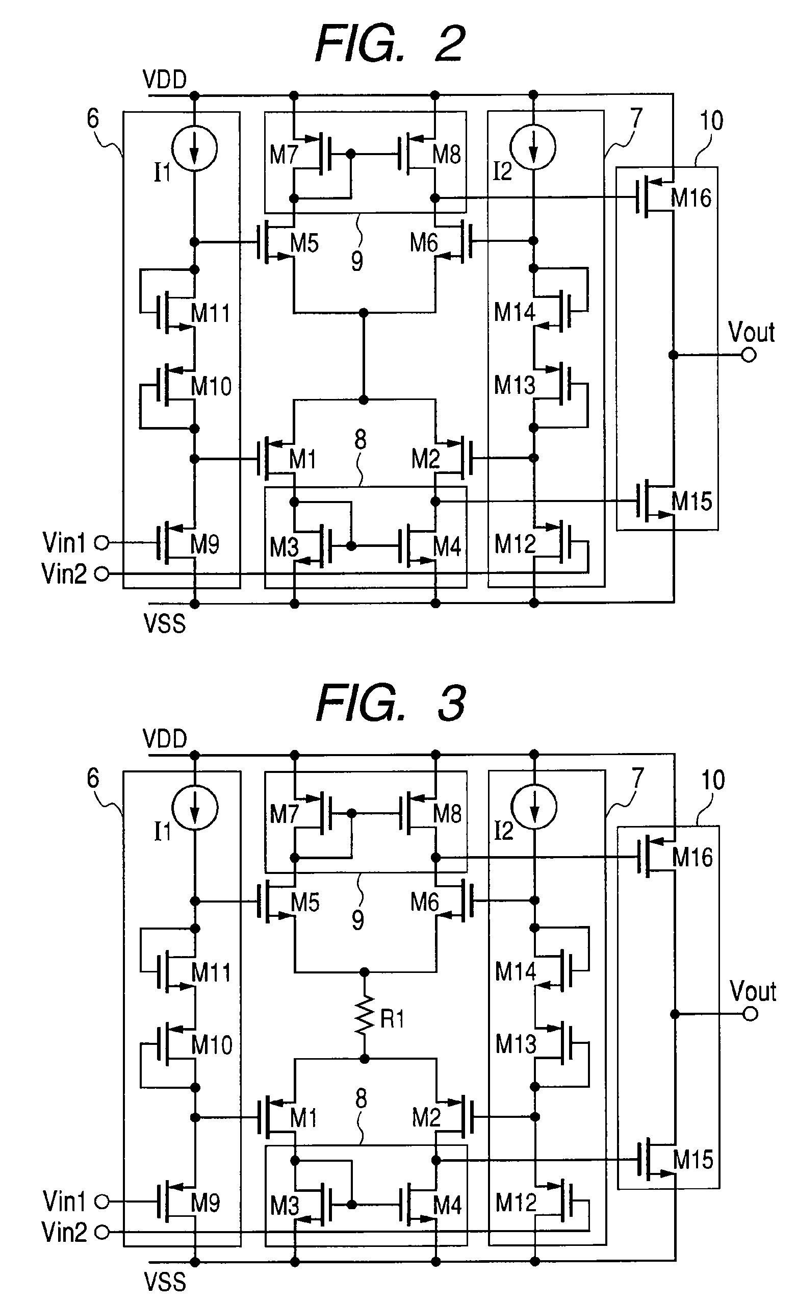
[0028]FIG. 2 shows a circuit diagram of an operational amplifier in this second embodiment of the present invention. PMOS transistors M1 and M2 make a differential transistor pair and NMOS transistors M5 and M6 make another differential transistor pair. The drains of those differential transistor pairs are connected to an active load 8 consisting of NMOS transistors M3 and M4 and another active load 9 consisting of NMOS transistors M7 and M8 respectively. The transistors M9, M10, and M11, as well as a current source I1 are combined to form a level shift circuit 6 while the transistors M12, M13, and M14, as well as a current source I2 are combined to form another level shift circuit 7. The M9 and M12 gates input signals Vin1 and Vin2 respectively and the NMOS transistor M15 and the PMOS transistor M16 are combined to form an output stage 10. And the M15 and M16 compose common source stage respectively to realize a high driving current and a wide output voltage range. Because the sour...

third embodiment

[0033]FIG. 3 shows an operational amplifier in this third embodiment of the present invention. In FIG. 3, a resistor R1 is used as a driving current control circuit. Because the resistor R1 is used in such a way, the current flowing in the subject differential transistor pair causes potential falling, which reduces the gate-source voltage of each transistor of the pair. Thus the current consumption can be reduced. In addition to the level shift circuits and differential transistor pairs, this embodiment can use another parameter that can control the driving current, thereby both the idle state current and the slew rate during operation can be controlled adjustably. If the R1 value increases, both the idle state current flowing in the differential transistor pair and the current flowing during operation can be reduced. While a resistor is used as a driving current control circuit in FIG. 2, the resistor may be replaced with another passive element, a transistor or the like.


PUM


Abstract

Disclosed herewith is a circuit system for improving a slew rate while reducing the power consumption in an operational amplifier that requires a comparatively high supply voltage (e.g., 5 V or upper) operation. The operational amplifier includes level shift circuits, differential pairs whose source connected serially, current voltage conversion circuit and output stage. The level shift circuits convert a differential input signal level and output to differential pairs. Combination of level shift circuit and differential pairs realize input signal difference detection and driving current control in the common circuit.

Description

CLAIM OF PRIORITY[0001]The present application claims priority from Japanese patent application JP 2008-009991 filed on Jan. 21, 2008, the content of which is hereby incorporated by reference into this application.FIELD OF THE INVENTION[0002]The present invention relates to an operational amplifier, more particularly to an operational amplifier that realizes high driving ability with a high supply voltage.BACKGROUND OF THE INVENTION[0003]Conventionally, there have been operational amplifiers, in each of which a detection circuit is connected to a current source in parallel and the current source supply is increased only when there is an input level difference detected at the detection circuit. (For such operational amplifiers, refer to JP-A-Hei 11-1360441, JP-A-2004-128815, and JP-A-Hei 11-88076.)[0004]Furthermore, there have also been other type operational amplifiers, in each of which the current source increases the current supply when there is an input level difference in a volt...

Claims


Application Information

Patent Timeline
Patent Type & Authority Patents(United States)
IPC IPC(8): H03F3/45
CPCH03F3/3022H03F3/45179H03F2203/45248H03F2203/45612
Inventor HAYASHI, YOSHIHIROYOSHINAGA, MASAKIMATSUMOTO, TAKASHI
Owner ABLIC INC
Learn More