Automated multiple voltage/power state design process and chip description system

Active Publication Date: 2011-07-19
SYNOPSYS INC
View PDF19 Cites 17 Cited by
  • Summary
  • Abstract
  • Description
  • Claims
  • Application Information

AI Technical Summary

Benefits of technology

[0012]An automated design process is also disclosed, comprising the steps of: creating a plurality of design objects, the design objects including a plurality of formal expressions for voltage effects in a design definition; processing a design definition according to the voltage effects design object; and generating a modified desi

Problems solved by technology

Specifically, such source files do not have a provision to express control of the design using voltage states.
Hence, it is not possible to simulate, synthesize, perform physical design or formally verify a design with multiple voltage states at the RTL and gate-level abstractions without manual intervention to compensate for the loss of voltage-related information.

Method used


Image

  • Automated multiple voltage/power state design process and chip description system
  • Automated multiple voltage/power state design process and chip description system
  • Automated multiple voltage/power state design process and chip description system

Examples


Embodiment Construction

[0023]The following serves as a glossary of terms as used herein:

[0024]CDS: Chip Description Language, as described below in this detailed description.

[0025]Constraints: commands used along with the RTL as inputs to various execution engines to provide additional specification not contained in the RTL.

[0026]Design tasks: tasks that are relevant for the implementation and verification of a design.

[0027]DFM: Design for Manufacturing, a rule and process set aimed at avoiding and reducing manufacturing errors.

[0028]DRC: Design Rule Checking, a process by which rules to ensure the safe realization of a design are checked.

[0029]LVS: Layout Verification to Schematic, a process by which polygon representations of the hardware are verified against a connectivity description.

[0030]Methods: procedures or functions that are declared and called by objects.

[0031]Object: An “object” is a collection of data fields (storage elements) and methods (associated functions).

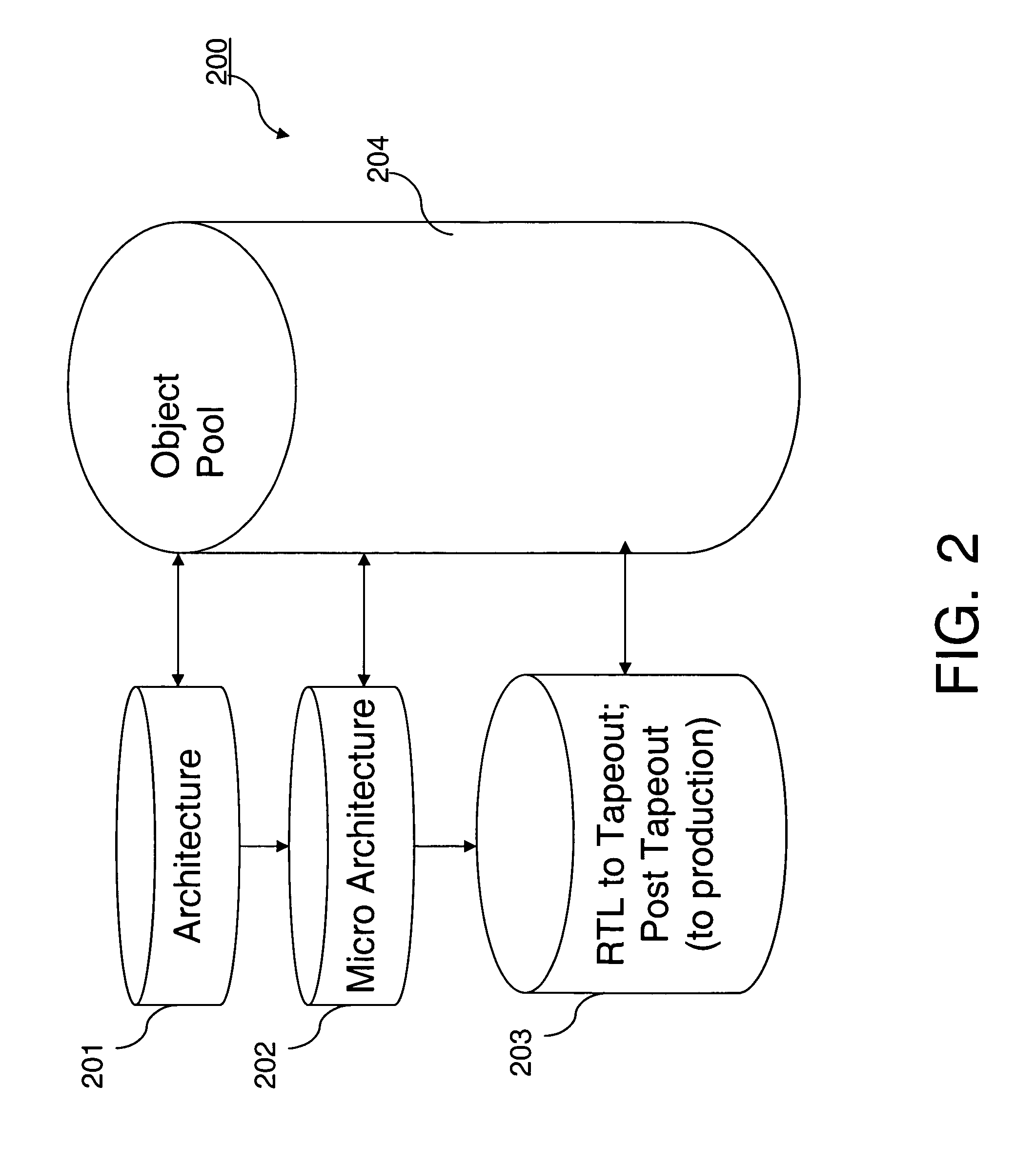
[0032]Object Pool: a plurality ...


PUM


Abstract

Systems and methods are disclosed herein which compensate for the loss in design information that occurs when the design is represented in traditional functional descriptions. An automated multiple voltage / power state design process includes creating a plurality of design objects; processing a design definition according to the voltage effects design object; and generating a modified design output such that communication between a plurality of design process steps, wherein the plurality of design process steps include a parsing step, a RTL simulation step, a synthesis step, a gate simulation step, formal verification step, and physical design and verification step in accordance with the voltage effects design object. A system for automating a multiple voltage / power state design process includes a design definition module; a parser module, a RTL simulation module, a synthesis module, a gate simulation module, and a formal verification module wherein the automation of a multiple voltage / power state design process is achieved. The system can include a physical design and verification module coupled to the synthesis module.

Description

RELATED APPLICATIONS[0001]This application claims priority to Provisional Application Ser. No. 60 / 589,330, filed Jul. 19, 2004, the benefit of the filing date of which is hereby claimed under 35 U.S.C. §119(e).BACKGROUND[0002]1. Field[0003]This invention relates to the art of electronic design automation (EDA), and more specifically to an automated design process and chip description system.[0004]2. Related Art[0005]In the art of semiconductor chip design, tools such as electronic design automation (EDA) are used to provide a means for automating the design of Integrated Circuits (IC) and Systems on a Chip (SoC) so that the design can be tested prior to the expensive process of implementing the design in silicon. Tools are also provide a means of automating the task(s) of preparing the design for manufacture on silicon.[0006]Hardware Description Languages (HDL) are used to model a chip and its functions. Existing HDL technology places the main functional description of Integrated Ci...

Claims


Application Information

Patent Timeline
IPC IPC(8): G06F17/50G06F9/455
CPCG06F17/504G06F30/3323
Inventor JADCHERLA, SRIKANTH
Owner SYNOPSYS INC
Why Eureka
Try Eureka