Light-emitting element, light-emitting device, lighting device, and electronic device

a technology of light-emitting elements and light-emitting devices, which is applied in the direction of semiconductor lamps, electrical devices, semiconductor devices, etc., can solve the problems of high voltage needed for driving the light-emitting element, acceleration of deterioration of the light-emitting element, and reducing power consumption, so as to achieve low power consumption and low power consumption

Active Publication Date: 2011-07-26
SEMICON ENERGY LAB CO LTD
View PDF17 Cites 34 Cited by
  • Summary
  • Abstract
  • Description
  • Claims
  • Application Information

AI Technical Summary

Benefits of technology

[0016]Furthermore, with the light-emitting element having the above structure, low driving voltage can be realized; therefore, low power consumption of a light-emitting device (e.g., an image display device or a light-emitting device) in which the light-emitting element is used can be realized. Thus, a light-emitting device in which the light-emitting element having the above structure is used and a lighting device and an electronic device in each of which the light-emitting device is used are also included as one embodiment of the present invention.
[0021]In addition, by manufacture of a light-emitting device using the above-described light-emitting element, the light-emitting device can have low power consumption. Furthermore, such a light-emitting device is applied to a lighting device and an electronic device, whereby the lighting device and the electronic device can have low power consumption.

Problems solved by technology

Supplying a large amount of current to the light-emitting layer is considered in order to increase emission luminance of such a light-emitting element; however, such a method hinders reduction of power consumption.
In addition, applying a large amount of current also leads to acceleration of deterioration of the light-emitting element.
However, in the light-emitting element having such a structure, mutual interaction occurs between the metal-doped layer and the charge-generation layer formed of the oxide at their interface and the interface has a high electric field; thus, high voltage is needed for driving the light-emitting element, unfortunately.

Method used


Image

  • Light-emitting element, light-emitting device, lighting device, and electronic device
  • Light-emitting element, light-emitting device, lighting device, and electronic device
  • Light-emitting element, light-emitting device, lighting device, and electronic device

Examples


embodiment 1

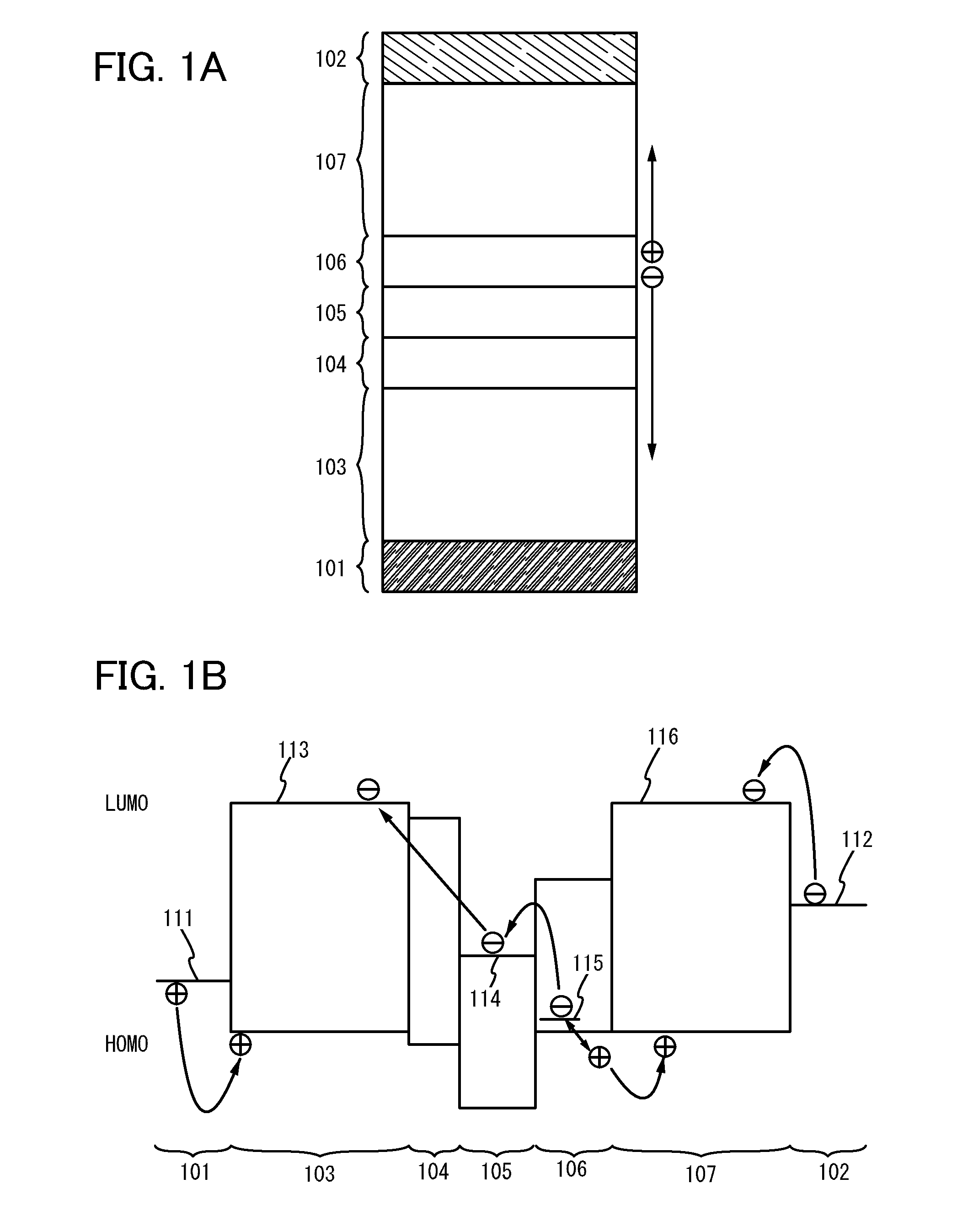
[0056]In Embodiment 1, one embodiment of a light-emitting element will be described with reference to FIGS. 1A and 1B.

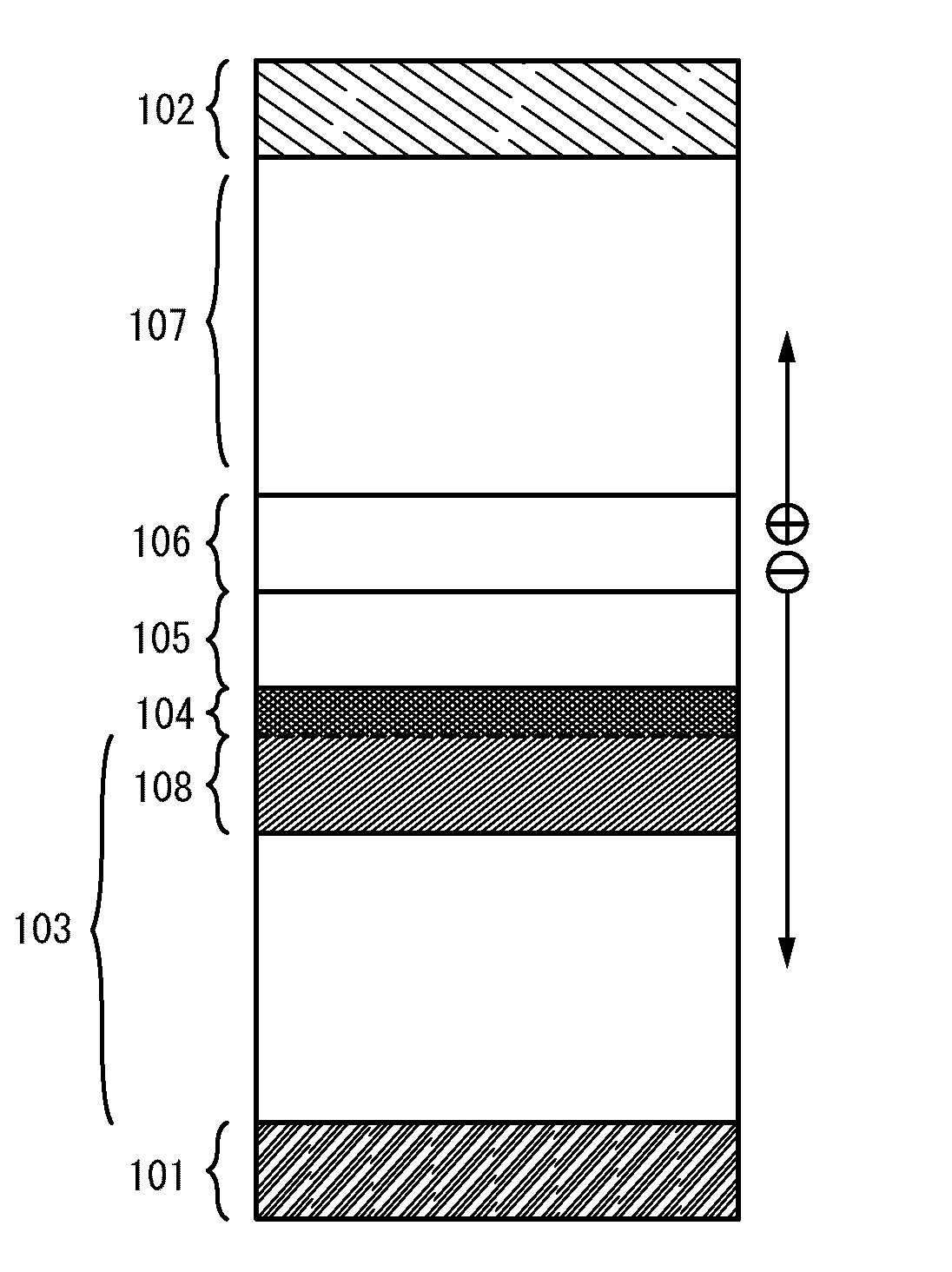
[0057]In an element structure illustrated in FIG. 1A, a first EL layer 103 and a second EL layer 107 each including a light-emitting region are sandwiched between a pair of electrodes (an anode 101 and a cathode 102), and between the first EL layer 103 and the second EL layer 107, an electron-injecting buffer 104, an electron-relay layer 105, and a charge production region 106 are stacked in this order from the anode 101 side.

[0058]The charge production region 106 is a region containing a material having a high hole-transporting property and an acceptor material, where holes and electrons that are carriers of the light-emitting element are produced. The holes produced in the charge production region 106 move to the second EL layer 107 while the electrons move to the electron-relay layer 105. Further, since the electron-relay layer 105 has a high electron-transporting...

embodiment 2

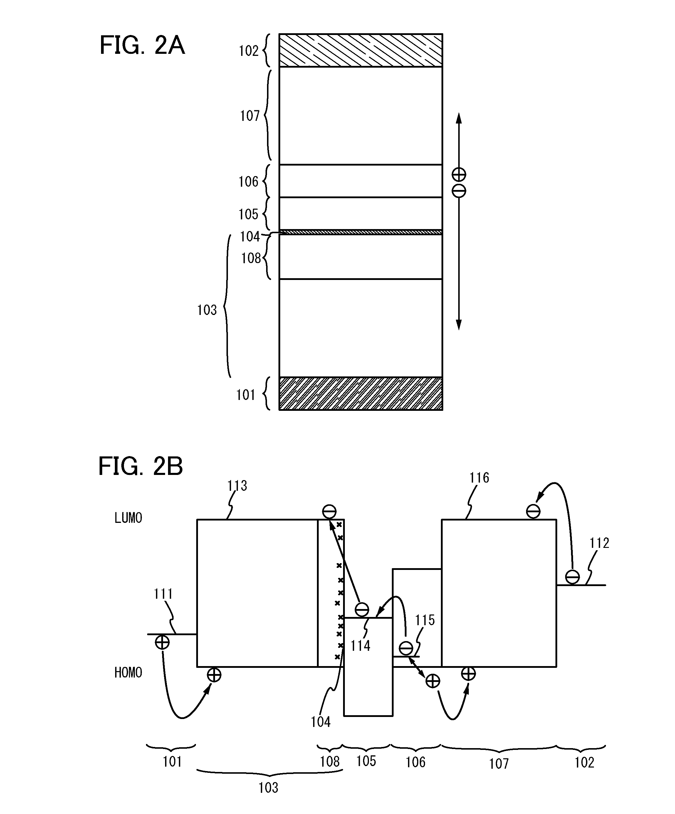
[0105]In Embodiment 2, an example of the light-emitting element included in the basic structure described in Embodiment 1 will be described with reference to FIGS. 2A and 2B. Specifically, a case where the electron-injecting buffer 104 has a single layer of an alkali metal, an alkaline earth metal, a rare earth metal, or a compound thereof will be described.

[0106]As illustrated in FIG. 2A, in a light-emitting element described in this embodiment, the first EL layer 103 and the second EL layer 107 each including a light-emitting region are sandwiched between a pair of electrodes (the anode 101 and the cathode 102), and between the first EL layer 103 and the second EL layer 107, the electron-injecting buffer 104, the electron-relay layer 105, and the charge production region 106 are stacked in this order from the anode 101 side.

[0107]The anode 101, the cathode 102, the first EL layer 103, the second EL layer 107, the charge production region 106, and the electron-relay layer 105 in Em...

embodiment 3

[0113]In Embodiment 3, an example of the light-emitting element included in the basic structure described in Embodiment 1 will be described with reference to FIGS. 3A and 3B. Specifically, a case where the electron-injecting buffer 104 of the light-emitting element described in Embodiment 1 contains a material having a high electron-transporting property and a donor material.

[0114]As illustrated in FIG. 3A, in a light-emitting element described in this embodiment, the first EL layer 103 and the second EL layer 107 each including a light-emitting region are sandwiched between a pair of electrodes (the anode 101 and the cathode 102), and between the first EL layer 103 and the second EL layer 107, the electron-injecting buffer 104, the electron-relay layer 105, and the charge production region 106 are stacked in this order from the anode 101 side. In addition, the electron-injecting buffer 104 contains a material having a high electron-transporting property and a donor material.

[0115]N...


PUM


Abstract

An object is to provide a light-emitting element which exhibits light emission with high luminance and can be driven at low voltage. Another object is to provide a light-emitting device or an electronic device with reduced power consumption. Between an anode and a cathode, n (n is a natural number of two or more) EL layers are provided, where between a first EL layer and a second EL layer, a first layer containing any of an alkali metal, an alkaline earth metal, a rare earth metal, an alkali metal compound, an alkaline earth metal compound, and a rare earth metal compound, a second layer containing a material having a high electron-transporting property in contact with the first layer, and a region containing a material having a high hole-transporting property and an acceptor material in contact with the second layer are provided in this order from the anode side.

Description

BACKGROUND OF THE INVENTION[0001]1. Field of the Invention[0002]The present invention hereinafter disclosed relates to a light-emitting element having a light-emitting layer between a pair of electrodes. In addition, the present invention relates to a light-emitting device in which the light-emitting element is used and a lighting device and an electronic device in each of which the light-emitting device is used.[0003]2. Description of the Related Art[0004]In recent years, a light-emitting element in which a light-emitting organic compound or a light-emitting inorganic compound is used as a light-emitting material has been actively developed. In particular, a light-emitting element called an electroluminescence (hereinafter, EL) element has a simple structure in which a light-emitting layer containing a light-emitting material is provided between electrodes, and has attracted attention as a next-generation flat panel display element because of its characteristics such as thinness, l...

Claims


Application Information

Patent Timeline
Patent Type & Authority Patents(United States)
IPC IPC(8): H01L27/15
CPCH01L51/5016H01L51/5036H01L51/504H01L51/5278H01L51/5004H01L51/0052H01L51/5012H01L51/0081H01L51/0072H01L51/007H01L51/0067H01L51/0054H01L51/0085H10K50/13H10K50/125H10K50/11H10K2101/10H10K50/19H10K85/622H10K85/654H10K85/6572H10K85/615H10K85/6565Y02B20/30H10K85/324H10K85/342H10K2101/40
Inventor NOWATARI, HIROMISEO, SATOSHIOHSAWA, NOBUHARUUSHIKUBO, TAKAHIROTSUTSUI, TETSUO
Owner SEMICON ENERGY LAB CO LTD
Why Eureka
Try Eureka