High speed probing apparatus for semiconductor devices and probe stage for the same

a probe stage and probe technology, applied in the direction of electronic circuit testing, measurement devices, instruments, etc., can solve the problem that the design of the device holder cannot be applied to the high speed testing system

Active Publication Date: 2011-07-26
STAR TECH INC
View PDF9 Cites 0 Cited by
  • Summary
  • Abstract
  • Description
  • Claims
  • Application Information

AI Technical Summary

Benefits of technology

[0008]One aspect of the present disclosure discloses a probe stage comprising a base, a retaining arm pivotally coupled with the base and having a retaining portion configured to retain at least one probe, and a stepper positioned on the base. In one embodiment of the present disclosure, the stepper is configured in response to an electric signal to move the probe downward through the retaining arm to contact a devi

Problems solved by technology

According to the prior art, the design of the device holder cannot be applied to the high speed testing system because the

Method used


Image

  • High speed probing apparatus for semiconductor devices and probe stage for the same
  • High speed probing apparatus for semiconductor devices and probe stage for the same
  • High speed probing apparatus for semiconductor devices and probe stage for the same

Examples


Embodiment Construction

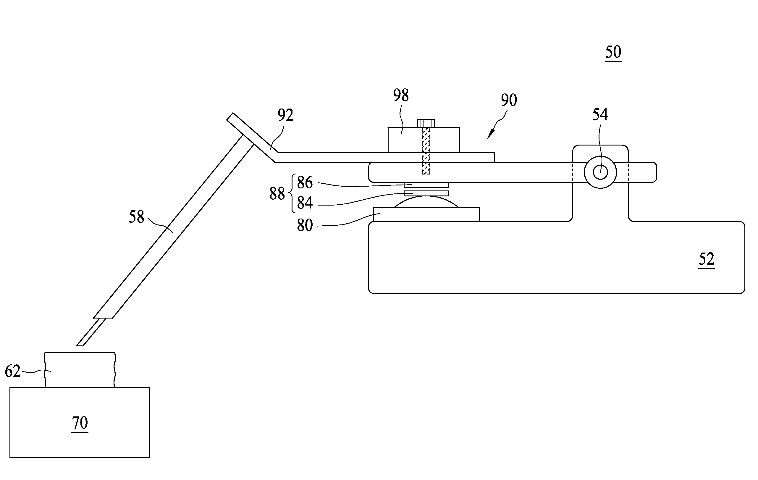
[0016]FIGS. 3 to 6 illustrate a probing apparatus 100 according to one embodiment of the present disclosure. The probing apparatus 100 comprises a housing 40, at least one probe stage 50 positioned in the housing 40 and configured to retain at least one probe 58, and a device holder 70 positioned in the housing and configured to receive at least one semiconductor device 62 under test. In one embodiment of the present disclosure, the housing 40 includes a body 42, a platen 44 positioned on the body 42 and a cover 46 configured to form a testing chamber 102 with the probe stage 50 and the device holder 70 positioned inside the testing chamber 102, wherein the probe stage 50 is positioned on the platen 44. In one embodiment of the present disclosure, the device holder 70 includes a movable stand 72 positioned in the housing 40, and a temperature-controller 74 such as a heater and / or cooler positioned in the device holder 70 and configured to control the temperature of the device holder...


PUM


Abstract

A probing apparatus for semiconductor devices includes a housing configured to define a testing chamber, a device holder positioned in the housing and configured to receive at least one device under test, and at least one probe stage positioned in the housing. In one embodiment of the present disclosure, the probe stage includes a base, a retaining arm pivotally coupled with the base and having a retaining portion configured to retain at least one probe, and a stepper positioned on the base. In one embodiment of the present disclosure, the stepper is configured in response to an electric signal to move the probe downward through the retaining arm to contact a device under test and to move the probe upward through the retaining arm to separate from the device under test such that the up-and-down movement of the probe can be performed at relatively high frequency of typically greater than six cycles per second. In one embodiment of the present disclosure, the stepper further equipped with a contact sensor configured to sense the contact of the probe to the device under test.

Description

BACKGROUND OF THE INVENTION[0001](A) Field of the Invention[0002]The present disclosure relates to a high speed probing apparatus for semiconductor devices and a probe stage for the same, and more particularly, to a probing apparatus for semiconductor devices and a probe stage for the same equipped with a high speed stepper configured to move the probe downward to contact a device under test and to move the probe upward to separate from the device under test and further equipped with a contact sensor configured to sense the contact of the probe to the device under test.[0003](B) Description of the Related Art[0004]Generally, it is necessary to test the electrical characteristics of semiconductor devices such as integrated circuit devices and light-emitting devices at the wafer level to check whether the semiconductor device satisfies the product specification. Semiconductor devices with electrical and optical characteristics satisfying the specification are selected for the subseque...

Claims


Application Information

Patent Timeline
IPC IPC(8): G01R31/20
CPCG01R1/07392G01R31/2891
Inventor LIU, YONG YU
Owner STAR TECH INC
Why Eureka
Try Eureka