Semiconductor device with three-dimensional field effect transistor structure

a three-dimensional structure and transistor technology, applied in the field of semiconductor devices, can solve the problems of insufficient consideration of three-dimensional fet, troublesome heat generation, heat dissipation, etc., and achieve the effect of efficiently dissipating the heat generated in the three-dimensional

Inactive Publication Date: 2011-08-02
RENESAS ELECTRONICS CORP
View PDF10 Cites 51 Cited by
  • Summary
  • Abstract
  • Description
  • Claims
  • Application Information

AI Technical Summary

Benefits of technology

[0012]Since the drain is generally connected to a metal interconnection, a method may be considered in which many contacts are provided on the drain for heat dissipation or that a metal interconnection having a large area is adopted. However, such method is not preferable since it increases the capacity of the drain.
[0016]According to the present invention, the heat generated in the three-dimensional FET can be efficiently dissipated.

Problems solved by technology

With regard to devices including the three-dimensional FET including the Fin FET or the planar SOI, the heat generation often becomes troublesome.
However, most of such investigations are directed to the planar SOI device, and the three-dimensional FET has not been sufficiently considered.
Generally, the heat dissipation is more important technical issue for the three-dimensional FET than the planar SOI device.
Accordingly, with such structure, since the heat from the metal interconnection is dissipated from a semiconductor layer through a contact plug, the amount of dissipated heat is limited by the thermal resistance of the contact plug.
As a result, heat exhaustion of the semiconductor layer is limited by the thermal resistance of the contact plug.
However, the present inventor has recognized that, in the FinFETs disclosed in Japanese Laid-Open Patent Application JP-P2006-19578A and JP-P2005-116969A, since a fin layer which a source, a channel and a drain thereon is isolatedly formed, it is difficult to dissipate the heat generated during the operation of the FinFET.
However, such method is not preferable since it increases the capacity of the drain.

Method used


Image

  • Semiconductor device with three-dimensional field effect transistor structure
  • Semiconductor device with three-dimensional field effect transistor structure
  • Semiconductor device with three-dimensional field effect transistor structure

Examples


first embodiment

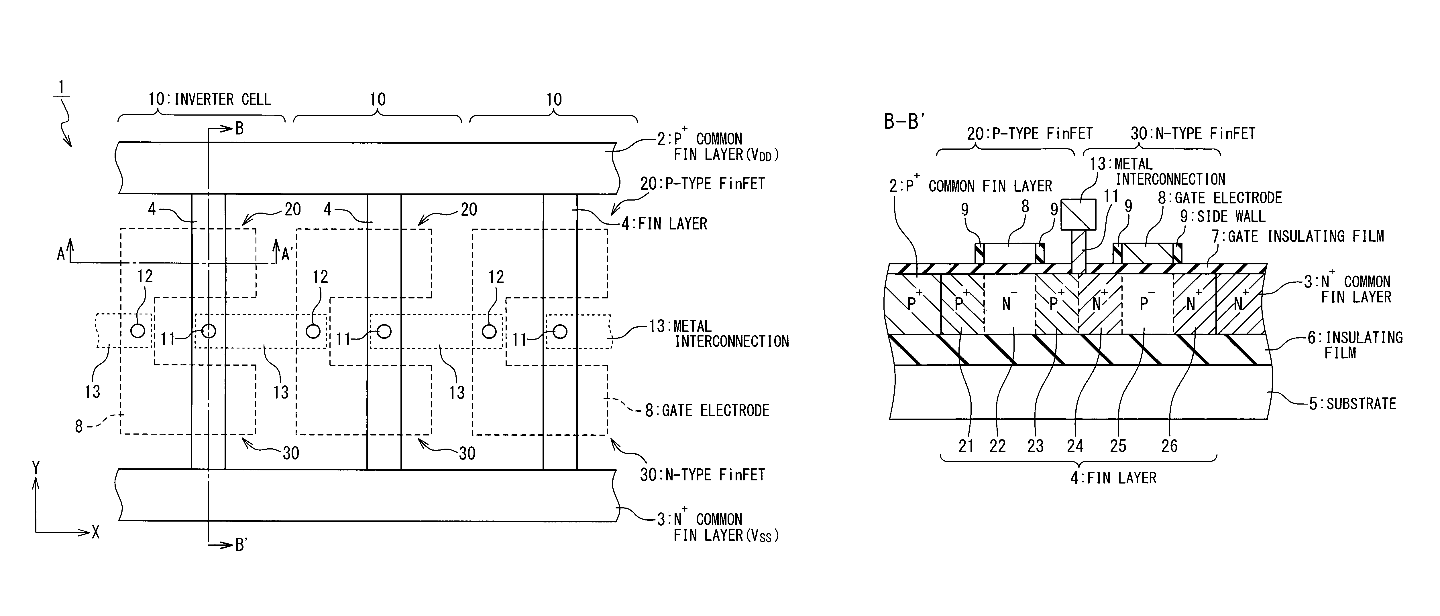
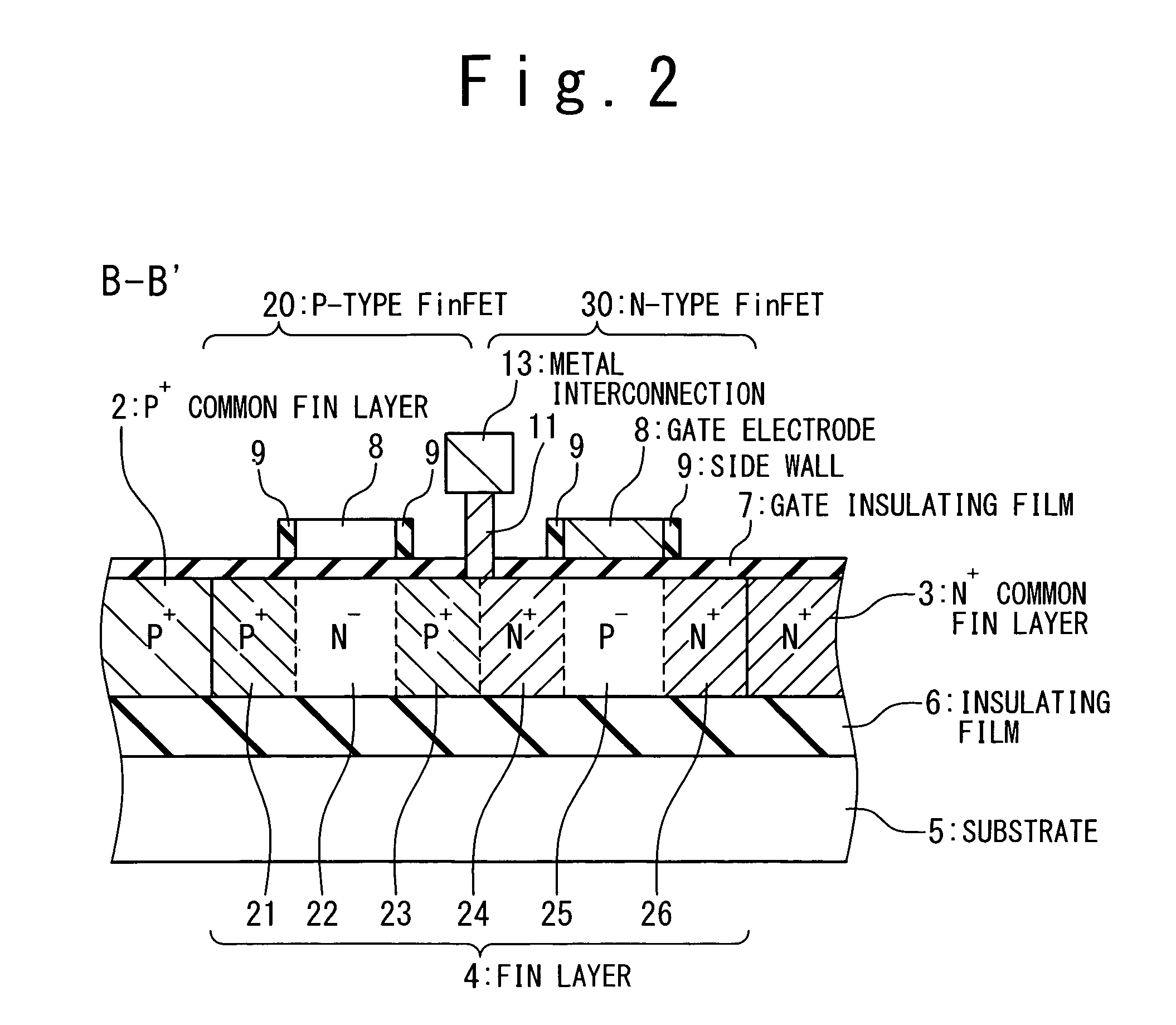
[0034]Hereinafter, a FinFET will be used for explanation as a typical example of three-dimensional FET. FIG. 1 is a plan view showing a layout of a semiconductor device 1 according to a first embodiment of the present invention. The semiconductor device 1 in FIG. 1 is formed of serially-connected three-stage inverter circuits 10. Each inverter circuit 10 has a P-type FinFET 20 and an N-type FinFET 30. In the semiconductor device 1 in FIG. 1, inverter circuits 10 are aligned in the X-axis direction and a signal is transmitted in a +X direction. A structure of the semiconductor device 1 will be described in detail below.

[0035]The semiconductor device 1 has a P+ common source semiconductor layer 2 and an N+ common source semiconductor layer 3 which extend in the X-axis direction. Here, the semiconductor layers can also be called as semiconductor blocks. The P+ common source semiconductor layer 2 is a semiconductor layer into which p-type impurities are doped at high concentration and i...

second embodiment

[0050]FIG. 5 is a plan view showing a configuration of a semiconductor device 1A according to a second embodiment of the present invention. Like the semiconductor device 1 of the first embodiment, the semiconductor device 1A of the second embodiment has serially-connected three-stage inverter circuits 10A. However, the shape of the fin layer and the gate electrode in the semiconductor device 1A of the second embodiment is different from those of the semiconductor device 1 of the first embodiment. In the first embodiment, the fin layer 4 is formed linearly along the Y-axis direction, while, in the second embodiment, a bent fin layer 4A is formed.

[0051]FIG. 6 is a plan view showing a configuration of the fin layer 4A. In the second embodiment, a part of the source region 21, the channel region 22 and a part of the drain region 23 of the P-type FinFET 20 are aligned in the X-axis direction, and a part of the drain region 24, the channel region 25 and a part of the source region 26 of t...

third embodiment

[0053]FIG. 7 is a plan view showing a configuration of a semiconductor device 1B according to a third embodiment. The semiconductor device 1B of the third embodiment functions as a NAND circuit having a P-type FinFETs 20A, 20B and N-type FinFETs 30A, 30B.

[0054]More specifically, the semiconductor device 1B has a fin layer 4B connecting the P+ common source semiconductor layer 2 to the N+ common source semiconductor layer 3. The fin layer 4B is divided into branches. Specifically, the fin layer 4B is formed of a part on which the P-type FinFET 20A is formed, a part on which the P-type FinFET 20B is formed and a part on which the N-type FinFETs 30A, 30B are serially arranged. One end of each of the parts on which P-type FinFETs 20A, 20B are formed is joined to the P+ common source semiconductor layer 2 and the other end of each of the parts is joined to one end of the part on which the N-type FinFETs 30A, 30B are formed. The other end of the part on which the N-type FinFETs 30A, 30B a...


PUM


Abstract

The semiconductor device includes first and second common source semiconductor layers respectively extending in a first direction, first and second logic gate circuits respectively composed of at least one three-dimensional P-type FET and a three-dimensional N-type FET. The sources of the three-dimensional P-type FETs in the first and second logic gate circuits are joined to the first common source semiconductor layer. The sources of the three-dimensional N-type FETs in the first and second logic gate circuits are joined to the second common source semiconductor layer. The semiconductor layers of the three-dimensional P-type and N-type FETs in the first logic gate circuit are joined in their drain side, and The semiconductor layers of the three-dimensional P-type and N-type FETs in the second logic gate circuit are joined in their drain side. The dissipation of the FinFET can be improved.

Description

INCORPORATION BY REFERENCE[0001]This patent application is based on Japanese Patent Application No. 2007-173807. The disclosure of the Japanese Patent Application is incorporated herein by reference.BACKGROUND OF THE INVENTION[0002]1. Field of the Invention[0003]The present invention relates to a semiconductor device, in particular, a semiconductor device having a three-dimensional structure MISFET (hereinafter, referred to a “three-dimensional FET”).[0004]2. Description of Related Art[0005]As a method of reducing the size of the MISFET (to achieve effects such as a suppression of short channel effect), the so-called three-dimensional FET is used for improving channel charge control capability of the gate electrode in place of a typical planar MISFET. The three-dimensional FET is a type of SOI (silicon on insulator) devices. The fin MISFET (FinFET) and the double gate FET (DG-FET) are typical three-dimensional FETs.[0006]As an example of the three-dimensional FET, an SRAM (static ra...

Claims


Application Information

Patent Timeline
Patent Type & Authority Patents(United States)
IPC IPC(8): H01L29/78
CPCH01L21/84H01L27/1203H01L29/785H01L2924/0002H01L2924/00
Inventor FURUTA, HIROSHI
Owner RENESAS ELECTRONICS CORP
Why Eureka
Try Eureka