

Peripheral device, integrated circuit for peripheral device and method for analyzing failure of peripheral device
a peripheral device and integrated circuit technology, applied in the field of peripheral devices, can solve the problems of reducing the number of peripheral devices, reducing the number of parts which are reducing the inspection or failure analysis of the peripheral device or the system lsi which is mounted on the peripheral device, so as to reduce the work failure that may occur in the process of alternately attaching the integrated circuit to the peripheral device, and narrow the range
- Summary
- Abstract
- Description
- Claims
- Application Information
AI Technical Summary
Benefits of technology
Problems solved by technology
Method used
Image


Examples
embodiment 1
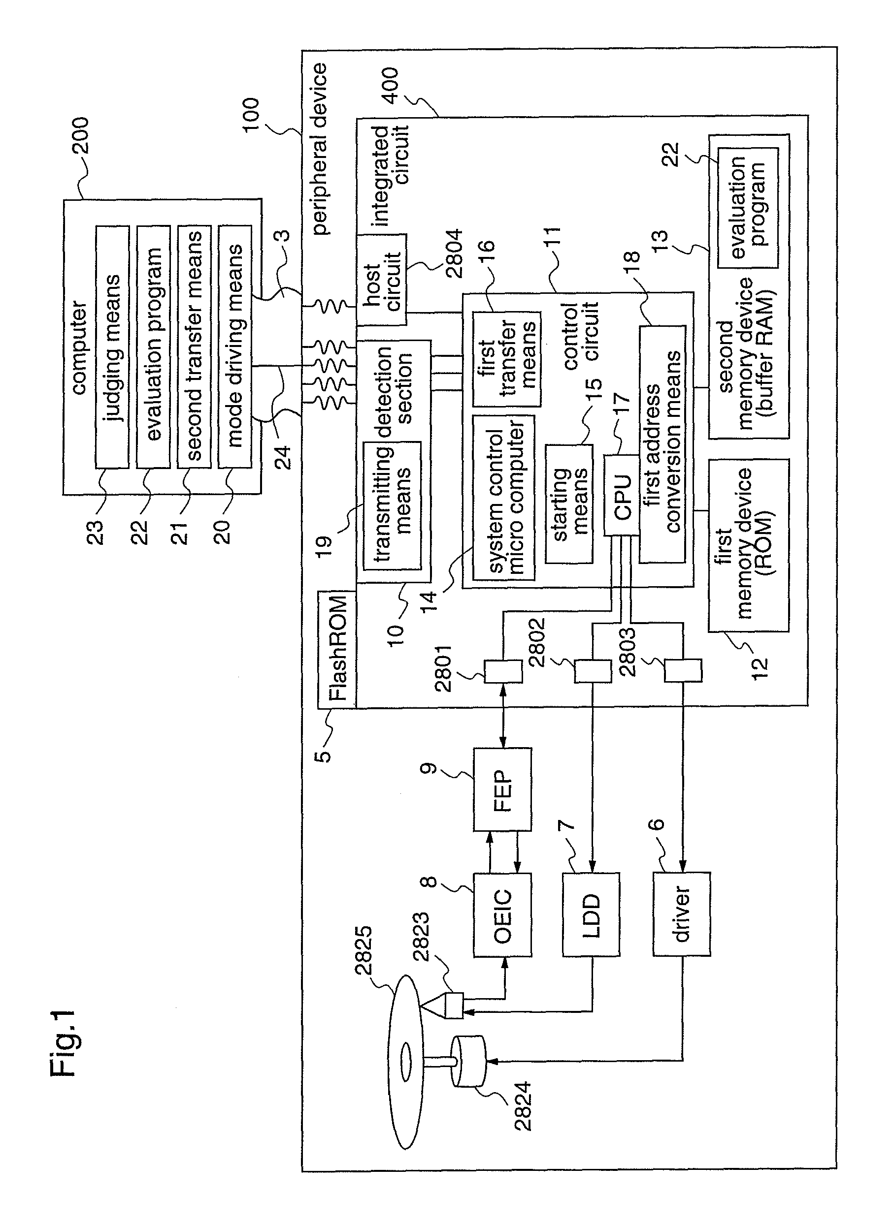
[0192]FIG. 1 is a diagram illustrating a construction example of a peripheral device and an integrated circuit for a peripheral device, and a computer which is connected to the peripheral device according to a first embodiment of the present invention. The same constitutional elements as those in the peripheral device and the integrated circuit as shown in FIG. 29 are designated by the same references, with their explanations omitted.
[0193]In FIG. 1, the peripheral device 100 and the computer 200 are connected to each other by an interface cable 3. Here, the interface cable 3 comprises concretely by interface cables such as ATA / ATAPI, SCSI, USB, IEEE1394, and Serial ATA. The interface cable 3 comprises one or more signal lines and one among them is a signal line 24 for transmitting a mode indicating signal which indicates whether the peripheral device 100 is operated in a normal mode or a test mode.
[0194]In addition, as the peripheral device 100, an optical disc device such as a DVD...
example 1
[0258]In the first method, as shown in FIG. 10, the bit which is not assigned to the ATA register in the ATA standards is employed as shown in FIG. 10. For example, the seventh bit obs of the Device / Head register, which is an abolished bit, is utilized. That is, when the chip select signal 41 is made one indicating the Device / Head register, address signal 42 are made CS0=Low, CS1=High, data signals are made as DA0=Low, DA1=DA2=High, 0b1xxxxxxx is written into the 7-th bit of the Device / Head register of ATA, that the signal of DD7=1 is driven is decoded and the test mode signal 34 is turned on in ON state to be outputted to the mode switching circuit 31.
example 2
[0259]In the second method, as shown in FIG. 11, when the register in the abolished region is employed in the address assignment for the ARTA register in the ATA standards, it is made such that CS0=Low, CS1=Low, DA0=DA1=DA2=High, and 0x01 is written into the data register of ATA, that the signal of DD0=1 and the signals of DD1 to DD15=0 are driven is decoded and the test mode signal 34 is turned on in ON state to be outputted to the mode switching circuit 31.
PUM
 Abstract
Description
Claims
Application Information