Low-temperature dielectric film formation by chemical vapor deposition

a dielectric film and low-temperature technology, applied in the field of low-temperature dielectric film deposition, can solve the problems of poor and generally uncontrollable nitrogen (n) incorporation into silicon oxide films, limit their use,

Inactive Publication Date: 2011-08-09
TOKYO ELECTRON LTD
View PDF9 Cites 255 Cited by
  • Summary
  • Abstract
  • Description
  • Claims
  • Application Information

AI Technical Summary

Benefits of technology

[0006]One embodiment of the invention provides a method for low-temperature CVD of silicon oxide films on a plurality of substrates in a batch processing system using dichlorosilane (DCS) and water vapor. The method includes positioning a plurality of substrates in a process chamber, heating the process chamber to a deposition temperature between 400° C. and less than 650° C., flowing a first process gas comprising water vapor into the process chamber, flowing a second process gas comprising dichlorosilane (DCS) into the process chamber, establishing a gas pressure of less than 2 Torr in the process chamber, and reacting the first and second process gases to thermally deposit a silicon oxide film on the plurality of substrates. Another embodiment further includes flowing a third process gas comprising nitric oxide (NO) gas into the process chamber while flowing the first process gas and the second process gas; and reacting the oxide film with the third process gas to form a silicon oxynitride film on the substrate.

Problems solved by technology

This CVD process requires relatively high substrate temperature (e.g., around 800° C.) which can limit its use when integrating silicon oxide films with advanced materials that require a low thermal budget.
Further, the use N2O gas as the oxidizing gas has been found to result in poor and generally uncontrollable nitrogen (N) incorporation into the silicon oxide films.
Low film deposition rates are thought to be due to a rate limiting DCS nucleation step on the oxide film that is due to absence of gas phase reactions between DCS and N2O.

Method used


Image

  • Low-temperature dielectric film formation by chemical vapor deposition
  • Low-temperature dielectric film formation by chemical vapor deposition
  • Low-temperature dielectric film formation by chemical vapor deposition

Examples


Embodiment Construction

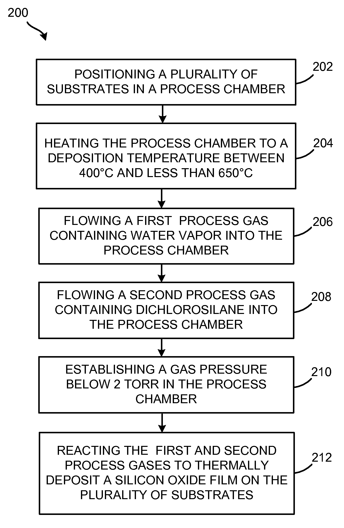
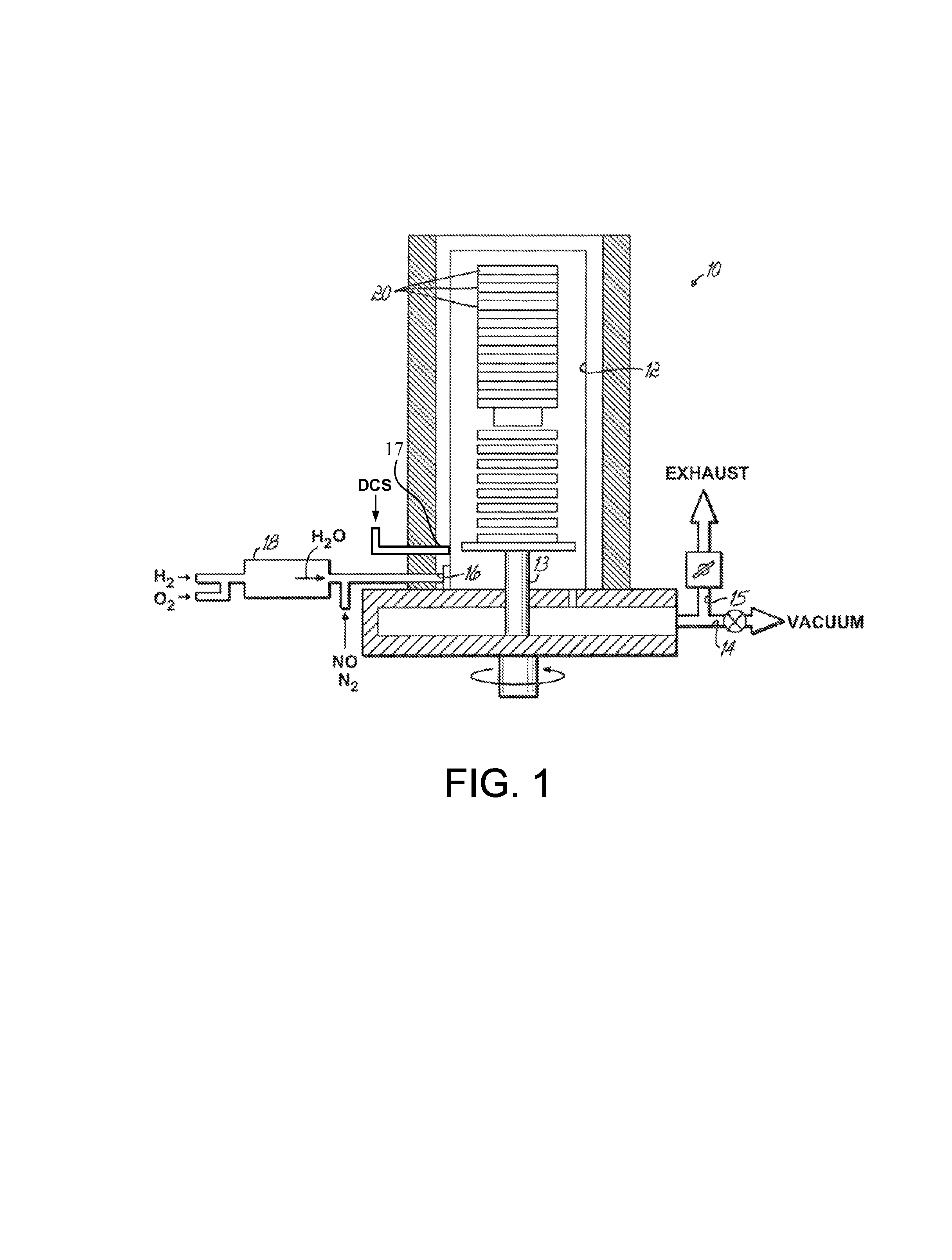
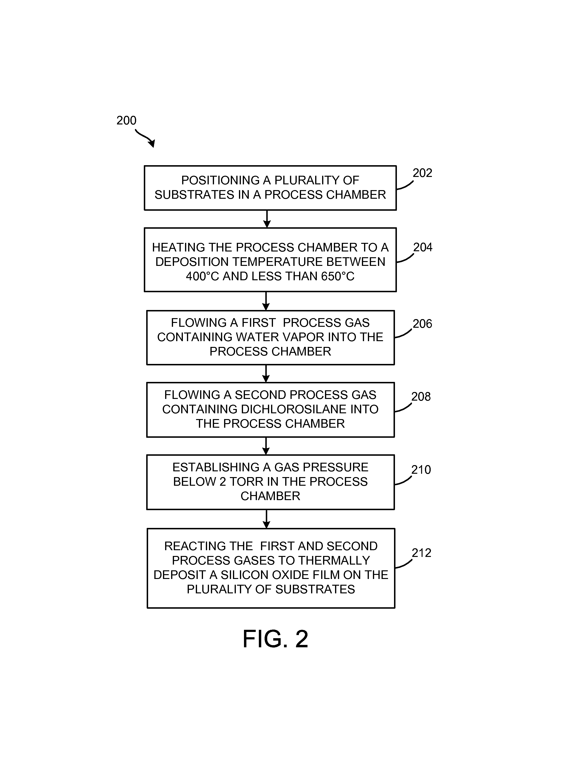
[0015]Embodiments of the invention provide a low-temperature deposition process for forming dielectric films for semiconductor devices. In one embodiment, a method is provided for non-plasma CVD of silicon oxide films using dichlorosilane (DCS) and water vapor. In another embodiment, a method is provided for non-plasma CVD of silicon oxynitride films using DCS, water vapor, and nitric oxide (NO) gas. Embodiments of the invention achieve high deposition rates of silicon dioxide and silicon oxynitride films with good material and electrical properties while utilizing lower deposition temperature than industry standard high-temperature oxide (HTO) processes that rely on the reaction of dichlorosilane (DCS) and nitrous oxide (N2O) on a substrate.

[0016]The inventors have realized that replacing a N2O oxidizer with a water vapor oxidizer, and optionally NO gas for forming silicon oxynitride films, allows for lowering the deposition temperature by greater than 100° C., greater than 200° C....


PUM


Abstract

A method for depositing a dielectric film on a substrate includes positioning a plurality of substrates in a process chamber, heating the process chamber to a deposition temperature between 400° C. and less than 650° C., flowing a first process gas comprising water vapor into the process chamber, flowing a second process gas comprising dichlorosilane (DCS) into the process chamber, establishing a gas pressure of less than 2 Torr, and reacting the first and second process gases to thermally deposit a silicon oxide film on the plurality of substrates. One embodiment further includes flowing a third process gas comprising nitric oxide (NO) gas into the process chamber while flowing the first process gas and the second process gas; and reacting the oxide film with the third process gas to form a silicon oxynitride film on the substrate.

Description

FIELD OF THE INVENTION[0001]The present invention relates to semiconductor substrate processing and, more particularly, to a method for low-temperature dielectric film deposition using a chlorinated silane and water vapor.BACKGROUND OF THE INVENTION[0002]In the formation of integrated circuits on the surface of a semiconductor substrate, oxide or oxynitride films are frequently grown or deposited over the surface of a crystalline substrate such as silicon. Industry standard processes for chemical vapor deposition (CVD) of high quality silicon oxide (SiOx, x≦2) films for semiconductor Flash memory and micro-feature sidewall applications are based on high-temperature reactions of dichlorosilane (DCS) and nitrous oxide (N2O), for example. The main benefits of this process include the ability to process multiple substrates simultaneously in a batch process, excellent electrical performance of the silicon oxide films, and relatively low wet etch rates of the films compared to other CVD f...

Claims


Application Information

Patent Timeline
Patent Type & Authority Patents(United States)
IPC IPC(8): H01L21/31
CPCH01L21/0214H01L21/02164H01L21/02271H01L21/3105H01L21/28202H01L21/28211H01L21/28185H01L21/28273H01L29/40114H01L21/02554
Inventor DIP, ANTHONYREID, KIMBERLY G
Owner TOKYO ELECTRON LTD
Why Eureka
Try Eureka