Photovoltaic devices having nanoparticle dipoles for enhanced performance and methods for making same

a technology of photovoltaic devices and dipoles, which is applied in the direction of nanotechnology, semiconductor devices, electrical devices, etc., can solve the problems of difficult to create a non-uniform distribution of ligands on the surface of nanoparticles, and achieve enhanced photovoltaic effects, increased time, and enhanced photovoltaic effects

Active Publication Date: 2011-08-09
LADARSYST INC
View PDF0 Cites 13 Cited by
  • Summary
  • Abstract
  • Description
  • Claims
  • Application Information

AI Technical Summary

Benefits of technology

[0005]The present invention provides, in one aspect, a photovoltaic device including nanoparticles having enhanced photovoltaic effect. A nonuniform distribution of electron rich and electron poor ligands on the nanoparticle surface induce an electric field in the nanoparticle. The induced dipole allows for the stabilization of multiple charges within the nanoparticle, providing increased time for allow for charge separation and extraction, thereby enhancing the photovoltaic effect and providing superior device performance.
[0008]The present invention provides, in one aspect, a method for producing a photovoltaic device having nanoparticles with an induced electric field. At least two challenges are overcome by the present method. First, it is difficult to create a nonuniform distribution of ligands on the surface of a nanoparticle. Second, even if such a nonuniform distribution were created, diffusive exchange would soon result in a uniform distribution. The present method provides a technique for producing a stable nonuniform distribution of different ligand types on the surface of nanoparticles in a photovoltaic device.

Problems solved by technology

First, it is difficult to create a nonuniform distribution of ligands on the surface of a nanoparticle.

Method used


Image

  • Photovoltaic devices having nanoparticle dipoles for enhanced performance and methods for making same
  • Photovoltaic devices having nanoparticle dipoles for enhanced performance and methods for making same
  • Photovoltaic devices having nanoparticle dipoles for enhanced performance and methods for making same

Examples


Embodiment Construction

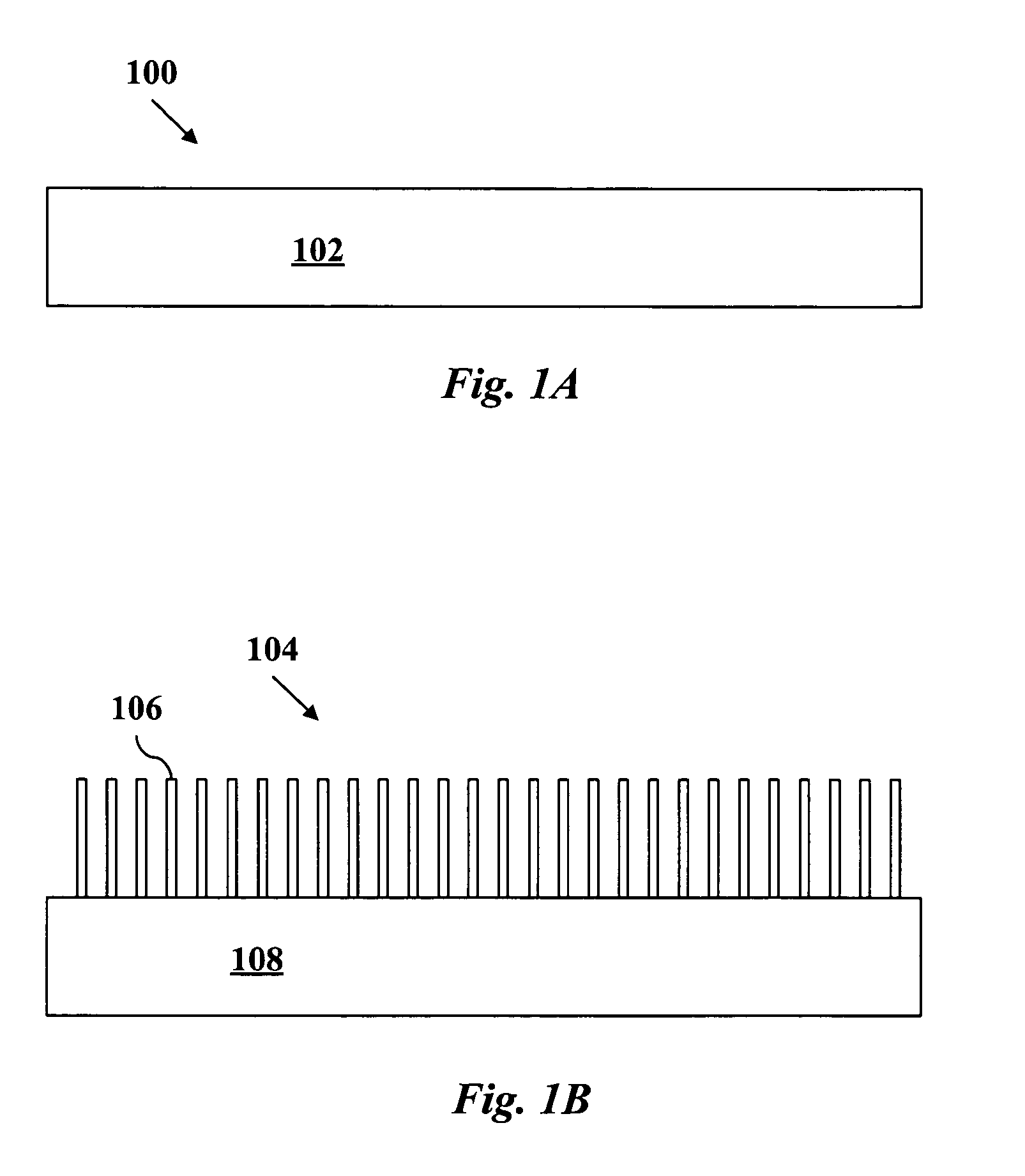
[0022]According to a preferred embodiment of the invention, a photovoltaic device is made by a collection of steps which will be described now in relation to the figures. In one step, a conductive substrate is surface functionalized with bifunctional ligands of a first type. In one embodiment, as shown in FIG. 1A, the conductive substrate 100 is a transparent conductive oxide substrate 102 such as TiO2. In a preferred embodiment, shown in FIG. 1B, the conductive substrate 104 is produced in a prior step by synthesizing metal oxide nanorods 106 on a transparent conductive oxide substrate 108.

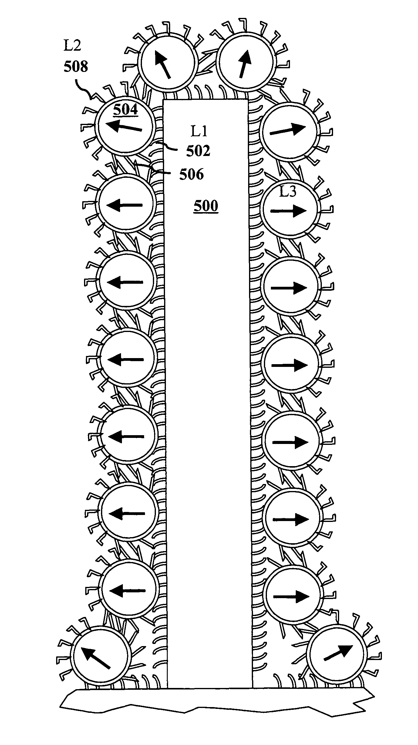
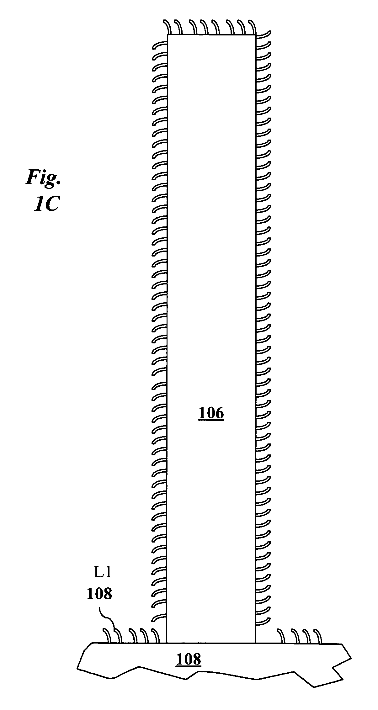
[0023]FIG. 1C illustrates a detail view of a surface functionalized nanorod 106 synthesized on transparent oxide substrate 108. The surface is functionalized with ligands 108 of the first type. Ligands 108 are may be, for example, ligands of the type shown in FIG. 2A, 2B, or 2C. In these figures, R represents an alkyl (C1-C6), an aromatic group (i.e., para-substituted phenyl group), or nothing. I...


PUM

PropertyMeasurementUnit
temperatureaaaaaaaaaa
conductiveaaaaaaaaaa
electric fieldaaaaaaaaaa

Abstract

A photovoltaic device has nanoparticles sandwiched between a conductive substrate and a charge selective transport layer. Each of the nanoparticles has a ligand shell attached to the nanoparticle core. A first type of ligand is electron rich and attached to one hemisphere of the nanoparticle core, while a second type of ligand is electron poor and attached to an opposite hemisphere of the core. Consequently, the ligand shell induces an electric field within the nanoparticle, enhancing the photovoltaic effect. The arrangement of ligands types on different sides of the nanoparticle is obtained by a process involving ligand substitution after adhering the nanoparticles to the conductive substrate.

Description

CROSS-REFERENCE TO RELATED APPLICATIONS[0001]This application claims priority from U.S. provisional patent application No. 60 / 983,642 filed 30 Oct. 2007, which is incorporated herein by reference.STATEMENT OF GOVERNMENT SPONSORED SUPPORT[0002]This invention was made with Government support under contract DE-PS36-07G097025 awarded by the Department of Energy. The US Government has certain rights in this invention.FIELD OF THE INVENTION[0003]The present invention relates generally to photovoltaic devices and methods for producing photovoltaic materials. More specifically, it relates to photovoltaic materials having nanoparticles and methods for making them.BACKGROUND OF THE INVENTION[0004]Photovoltaic materials such as solar cells operate on the basis of the photovoltaic effect. In the case of photovoltaic materials including nanoparticles, it is known that incident light can produce multiple excitons within a nanoparticle. However, to take advantage of multiple excitons to produce in...

Claims


Application Information

Patent Timeline
Patent Type & Authority Patents(United States)
IPC IPC(8): H01L31/00H01L21/00
CPCH01L31/0352H01L31/035281H01L31/0392Y02E10/50H01L31/03925Y10S977/773Y10S977/778Y10S977/813
Inventor WILLIAMS, GEORGE M.SCHUT, DAVID M.STONAS, ANDREAS
Owner LADARSYST INC
Why Eureka
Try Eureka