Pt-GFW/SiO2/n-Si heterojunction material and preparation method thereof

A heterojunction, pt-gfw technology, applied in the field of materials, can solve problems such as weak response to visible light, and achieve the effects of improved photovoltaic effect, superior performance and simple preparation

Active Publication Date: 2015-09-02
CHINA THREE GORGES UNIV
View PDF3 Cites 0 Cited by
  • Summary
  • Abstract
  • Description
  • Claims
  • Application Information

AI Technical Summary

Problems solved by technology

The device mentioned in the literature has a weak response to visible light

Method used


Image

  • Pt-GFW/SiO2/n-Si heterojunction material and preparation method thereof
  • Pt-GFW/SiO2/n-Si heterojunction material and preparation method thereof
  • Pt-GFW/SiO2/n-Si heterojunction material and preparation method thereof

Examples


Embodiment 1

[0024] The invention improves the response of the graphene solar cell to visible light at room temperature.

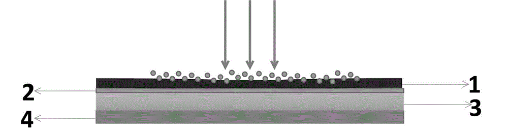
[0025] First, heat the copper grid from room temperature to 1000°C in an argon atmosphere for 80 minutes, then pass hydrogen gas at 1000°C for 30 minutes, and pass argon, hydrogen, and methane at a ratio of 200:2:30 at 1000°C. , reacted for 20 minutes. Under argon protection, cool down to room temperature. The copper mesh on which the graphene mesh was grown was etched with ferric nitrate solution and washed three times with deionized water. The wafers were then ultrasonically cleaned two to three times with acetone, and then cleaned with hydrofluoric acid. The cleaned graphene mesh was then transferred to a silicon wafer. Stand still at room temperature for 15 hours to form a naturally oxidized silicon dioxide layer where the silicon of the device is not well connected to the graphene network, and thus assemble into a graphene solar cell in the usual sense.

[002...

Embodiment 2

[0034] The experiment is to first heat the copper mesh from room temperature to 1000°C in an argon atmosphere for 60 minutes, then pass hydrogen gas at 1000°C for 30 minutes, and pass argon and hydrogen at a ratio of 200:2:30 at 1000°C. , methane, reacted for 20 minutes. Under argon protection, cool down to room temperature. The copper mesh on which the graphene mesh was grown was etched with ferric nitrate solution and washed three times with deionized water. The wafers were then ultrasonically cleaned two to three times with acetone, and then cleaned with hydrofluoric acid. The cleaned graphene mesh was then transferred to a silicon wafer. Stand still at room temperature for 15 hours to form a naturally oxidized silicon dioxide layer where the silicon of the device is not well connected to the graphene network, and thus assemble into a graphene solar cell in the usual sense.

[0035] The thickness of the silicon oxide layer may be 1.5-2.5 nanometers.

[0036] The thickne...

Embodiment 3

[0043] The invention improves the response of the graphene solar cell to visible light at room temperature.

[0044] First, heat the copper grid from room temperature to 1000°C in an argon atmosphere for 80 minutes, then pass hydrogen gas at 1000°C for 30 minutes, and pass argon, hydrogen, and methane at a ratio of 200:2:30 at 1000°C. , reacted for 20 minutes. Under argon protection, cool down to room temperature. The copper mesh on which the graphene mesh was grown was etched with ferric nitrate solution and washed three times with deionized water. The wafers were then ultrasonically cleaned two to three times with acetone, and then cleaned with hydrofluoric acid. The cleaned graphene mesh was then transferred to a silicon wafer. Stand still at room temperature for 15 hours to form a naturally oxidized silicon dioxide layer where the silicon of the device is not well connected to the graphene network, and thus assemble into a graphene solar cell in the usual sense.

[004...


PUM

PropertyMeasurementUnit
thicknessaaaaaaaaaa
thicknessaaaaaaaaaa
thicknessaaaaaaaaaa

Abstract

The invention discloses a Pt-GFW/SiO2/n-Si heterojunction material and a preparation method thereof. After a graphene network (GFW) grown by using a chemical vapor deposition (CVD) method is transferred onto an n-type silicon (n-Si (100)) substrate, a heterojunction thin film material having a white light photovoltaic effect is formed. By the way of laser irradiation of a high platinic acid solution to load platinum nanoparticles, the platinum nanoparticles are loaded onto the surface of a GFW/n-Si device. According to the invention, the platinum-loaded graphene, silicon solar cells are irradiated at room temperature and with a simulated solar light source of 100mW/cm2, the open-circuit photo voltage of the device is increased from 474mV to 545mV, the short-circuit photocurrent is increased from 18.2mA/cm2 to 19.6mA/cm2, the fill factor is increased from 42.8% to 51.2% or more, and the photoelectric conversion efficiency is increased from 3.69% to 5.48%. The adopted method is excellent in performance, low in cost and easy in preparation; and different from methods in the prior art in which nitrotoluene is used as a solvent, the method uses deionized water as a solvent, and is an excellent method which can enhance visible light sensor materials and have potential photovoltaic device performance.

Description

technical field [0001] The invention belongs to a method for improving the performance of thin-film solar cell materials and photoelectric devices, and belongs to the field of material technology, in particular to a method for improving the performance of graphene and silicon heterojunction solar cells Pt-GFW / SiO 2 / n-Si heterojunction material and its preparation method. Background technique [0002] Energy shortage and environmental issues are getting more and more attention. Photovoltaic power generation has attracted much attention because it can directly convert solar light energy into electrical energy. Research on photovoltaic power generation technology began more than 100 years ago. In 1839, the French physicist A.E. Becqurel accidentally discovered that a voltaic battery composed of two pieces of metal intruding into the solution would generate an additional voltaic potential when illuminated. He called this phenomenon "photovoltaic". Effect" (photovoltaic effect...

Claims


Application Information

Patent Timeline
Patent Type & Authority Applications(China)
IPC IPC(8): H01L31/0745H01L31/028H01L31/18B82Y40/00
CPCB82Y40/00H01L31/028H01L31/0745H01L31/1804Y02E10/547Y02P70/50
Inventor 谭新玉康喆田丹妮肖婷向鹏姜礼华
Owner CHINA THREE GORGES UNIV
Why Eureka
Try Eureka