A kind of graphene/si p-n double junction solar cell and preparation method thereof

A technology of solar cells and graphene, applied in the field of solar cells, can solve problems such as difficult control and complexity, achieve high repeatability, fast response speed, and improve the effect of photovoltaic effect and conversion efficiency

Inactive Publication Date: 2015-10-28
SUZHOU UNIV OF SCI & TECH
View PDF5 Cites 0 Cited by
  • Summary
  • Abstract
  • Description
  • Claims
  • Application Information

AI Technical Summary

Problems solved by technology

Many methods for preparing graphene are relatively complicated, the whole process is difficult to control, and only a small amount of graphene nano-film can be produced, while the graphene sheet prepared by chemical vapor deposition has good electronic properties and is suitable for the application of transistors, solar energy Batteries and other optoelectronic devices

Method used


Image

  • A kind of graphene/si p-n double junction solar cell and preparation method thereof
  • A kind of graphene/si p-n double junction solar cell and preparation method thereof
  • A kind of graphene/si p-n double junction solar cell and preparation method thereof

Examples


Embodiment 1

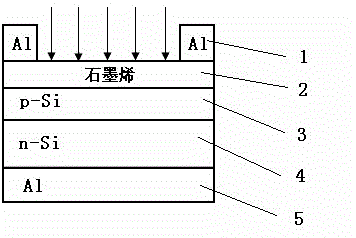
[0024] See attached figure 1 , which is a schematic diagram of the structure of the graphene / p-n Si double-junction solar cell provided in this embodiment, its structure is followed by Al electrode 1, graphene film layer 2, p-type Si conductive layer 3, n-type Si conductive layer 4 and Al Electrode 5.

[0025] B doping is performed on the upper surface of the n-type silicon wafer (111) to obtain a p-type conductive layer 3; a p-n junction is formed between the p-type conductive layer and the n-type conductive layer 4 of the substrate. On the upper surface of the p-type conductive layer, a graphene film 2 with a thickness of one to more than ten atomic layers (10-20nm) is grown by chemical vapor deposition. The junctions together form a double junction, and the Al electrode 5 is vapor-deposited on the lower surface of the n-silicon wafer to obtain a graphene / p-n Si double-junction solar cell.

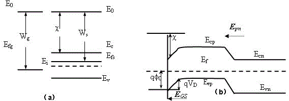
[0026] See attached figure 2 , which is a schematic diagram of the energy band s...


PUM

PropertyMeasurementUnit
thicknessaaaaaaaaaa
thicknessaaaaaaaaaa
transmittivityaaaaaaaaaa

Abstract

The invention discloses a graphene / Sip-n double-junction solar cell and a preparing method thereof. The Si surface of an n-type silicon slice (111) is mixed with B to achieve a p-type conducting layer, a Sip-n junction is formed between the p-type conducting layer and a liner n-type conducting layer. Under the condition that CH4 serves as reactant gas, Ar diluent gas is under the temperature of 900-1000 DEG C, a mode of chemical vapor deposition is adopted, a graphene thin layer with the thickness of 10-20 nm is generated on the surface of the p-type conducting layer, the graphene thin layer and the Sip-n junction are combined to form a schottky junction, and a double-junction solar cell is formed by the schottky junction and the Sip-n junction. Due to the fact that a heterojunction between the graphen and the Sip-n junction in the solar cell has important functions of transparent electric conduction, absorbing sunlight and collecting photoproduction electron-hole, conversion efficiency of luminous energy of the graphene / Sip-n double-junction solar cell reaches 2.26%.

Description

technical field [0001] The invention relates to a solar cell, in particular to a graphene / Si p-n junction double-junction solar cell and a preparation method thereof. Background technique [0002] Graphene is a single-layer two-dimensional (2D) honeycomb crystal with a thickness of only 0.35 nm and densely stacked carbon atoms in hexagonal cells. Graphene, which is composed of a single layer of carbon atoms, has been recognized as the thinnest, hardest, and fastest electron-conducting material in the world. Graphene is a semiconductor without an energy gap, and the mobility of carriers in it is as high as 2×10 5 cm 2 / v, 100 times higher than electron mobility in silicon. Graphene also has good optical properties, with a visible light transmittance as high as 98.5%, and can be used in transparent conductive films and solar cells. Research on graphene solar cells has also been reported, but its energy conversion efficiency is generally relatively low. For example (C. Xie...

Claims


Application Information

Patent Timeline
Patent Type & Authority Patents(China)
IPC IPC(8): H01L31/078H01L31/0224H01L31/18
CPCY02E10/50Y02P70/521Y02P70/50
Inventor 马锡英顾伟霞沈娇艳唐运海
Owner SUZHOU UNIV OF SCI & TECH
Why Eureka
Try Eureka