
Jig for detecting position

a position detection and detecting jig technology, applied in the field of position detection jigs, can solve the problems of inability to load the trajectory-detecting wafer into the apparatus, inability to properly process the wafer, and inability to properly deliver the wafer

Inactive Publication Date: 2011-08-09
TOKYO ELECTRON LTD
View PDF10 Cites 17 Cited by
  • Summary
  • Abstract
  • Description
  • Claims
  • Application Information

AI Technical Summary

Benefits of technology

The present invention provides a position detecting jig for accurately and stably detecting the transfer point of a transfer arm. The jig includes an electrostatic capacitance sensor with a detection electrode and a guard electrode for blocking an electric field. The detection electrode is installed on the rear surface of the main body of the jig, while the guard electrode is installed on the front surface. The electrostatic capacitance sensor is connected to a control circuit installed on the front surface of the main body. The rear surface wiring and the front surface wiring are connected with each other by a connection wiring extended in a thickness direction from the rear surface of the main body toward the front surface. The front surface wiring is covered by a front surface wiring guard electrode. The length of the connection wiring guard electrode is at least three times as long as the unguarded portion of the connection wiring against the electric field. The detection electrode may have a plurality of electrode portions, which are surrounded by individual lateral guard electrodes. The position alignment of the transfer arm can be performed properly by detecting the transfer point of the transfer arm accurately and stably, which allows for proper processing of the substrate using the transfer arm.

Problems solved by technology

However, in case that the wafer is not transferred to a preset position in each apparatus, the delivery of the wafer may not be performed properly or processing of the wafer may not be carried out properly because of a deviation of a processing position of the wafer, for example.
For this reason, as for an apparatus having a reduced opening size due to miniaturization of the wafers being transferred, it is impossible to load the trajectory-detecting wafer into the apparatus, and to adjust the position thereof properly, either.
However, when the electrostatic capacitance sensor is used on the position detecting wafer, there is a likelihood that the electrostatic capacitance may not be detected accurately and stably by being affected by, for example, an electric field if a generation source of the electric field is located nearby.
In such case, an accurate detection of the transfer point of the transfer arm becomes impossible to achieve.

Method used


Image

  • Jig for detecting position
  • Jig for detecting position
  • Jig for detecting position

Examples


experiment example 1

[0080]Hereinafter, there was conducted an evaluation of the effect of setting the length of the connection wiring guard electrode from the connection wiring to be at least three times as long as the length of the connection wiring's unguarded portion from the electric field in the position detecting jig in accordance with the present disclosure.

[0081]In the present experiment example, a structure 200, as shown in FIG. 15, having a jig 210 serving as the position detecting wafer S in accordance with the present embodiment was used. FIG. 15 provides a cross sectional view of the structure 200. The jig 210 includes a conductor 211 as the connection wiring 61, a conductor 212 as the guard electrode 112, a conductor 213 as the guard electrode 110a, a dielectric 214 as the substrate H, and a dielectric 215 as the layer N. The conductors 211 to 213 and the dielectrics 214 and 215 have the substantially identical configuration as that of the position detecting wafer S shown in FIG. 13 in ac...


PUM


Abstract

A transfer point of a transfer arm is detected accurately and stably by using a position detecting wafer having an electrostatic capacitance sensor. A position detecting wafer S is formed in a wafer shape transferable by a transfer arm 20 and includes an electrostatic capacitance sensor 50 for detecting a relative position with respect to a reference object by detecting an electrostatic capacitance in relation with the reference object for a position detection. The electrostatic capacitance sensor 50 includes a detection electrode 52 for forming the electrostatic capacitance in relation with the reference object, and the detection electrode 52 is installed on a rear surface of a main body of the wafer shape. Installed on the main body is a guard electrode 100 covering the detecting electrode 52 when viewed from a front surface thereof, for blocking an electric field oriented toward the detection electrode 52 from the front surface.

Description

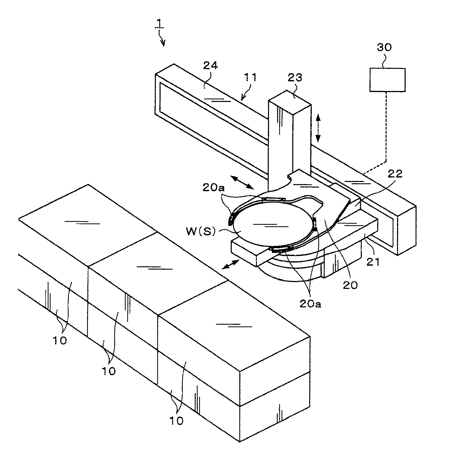
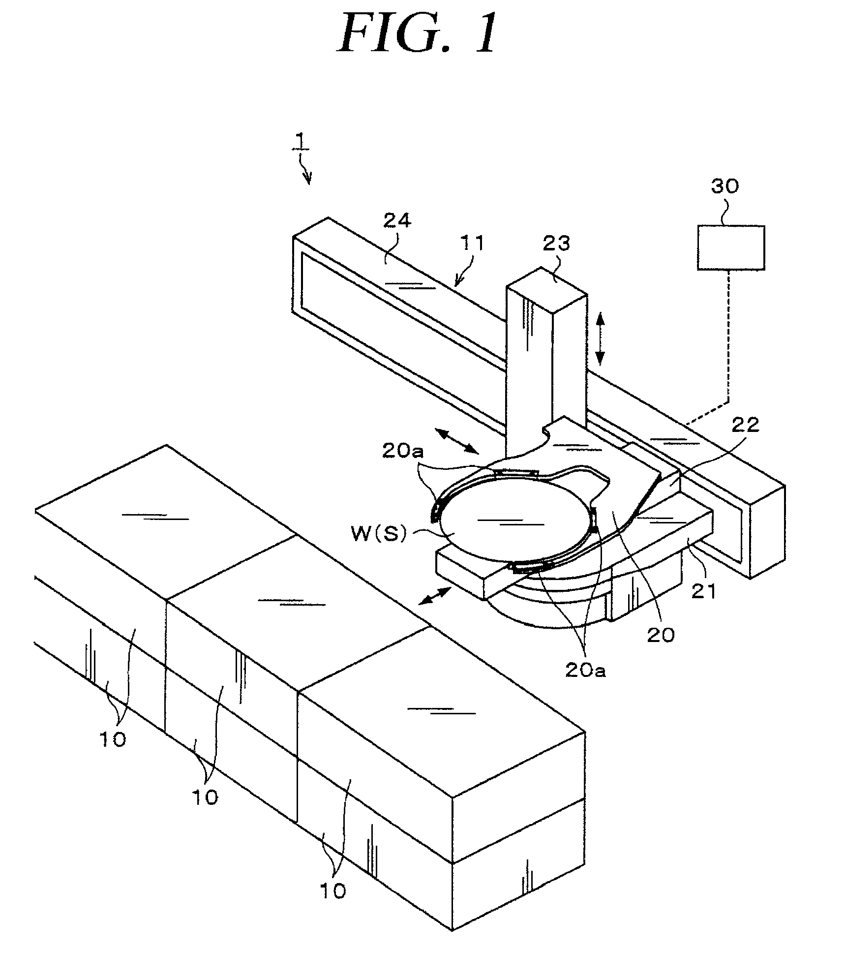
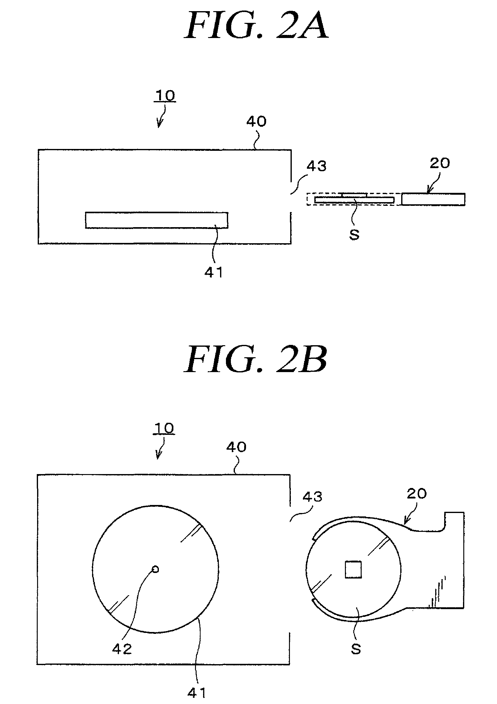
FIELD OF THE INVENTION[0001]The present disclosure relates to a position detecting jig for detecting a transfer point of a transfer arm for holding and transferring a substrate.BACKGROUND OF THE INVENTION[0002]For example, in a manufacturing process of semiconductor devices, a photolithography process is performed by a coating and developing system including a plurality of apparatuses such as a resist coating apparatus, a developing apparatus, a heat treating apparatus and the like. The coating and developing system has a transfer mechanism for transferring a wafer to each of the apparatuses.[0003]The transfer mechanism has a transfer arm for holding the wafer thereon, and, for example, the transfer arm moves three-dimensionally in forward-backward, left-right, and up-down directions to transfer the wafer to each apparatus.[0004]However, in case that the wafer is not transferred to a preset position in each apparatus, the delivery of the wafer may not be performed properly or proces...

Claims


Application Information

Patent Timeline
Patent Type & Authority Patents(United States)
IPC IPC(8): G01R29/12
CPCH01L21/67259H01L21/68
Inventor MATSUMOTO, TOSHIYUKIMINAMI, TOMOHIDEMAHARA, KOJIDOUKI, YUICHI
Owner TOKYO ELECTRON LTD
Learn More