Microscope and inspection apparatus

a technology of inspection apparatus and microscope, which is applied in the field of microscopes, can solve the problems of reducing image quality and increasing the leakage of electric charges between adjacent pixels, and achieve the effect of detecting the defect existing in the sample more accurately

a technology of inspection apparatus and microscope, which is applied in the field of microscopes, can solve the problems of reducing image quality and increasing the leakage of electric charges between adjacent pixels, and achieve the effect of detecting the defect existing in the sample more accurately

US20130188251A1Inactive Publication Date: 2013-07-25LASERTEC CORP

Image

  • Microscope and inspection apparatus
  • Microscope and inspection apparatus
  • Microscope and inspection apparatus

Examples


Embodiment Construction

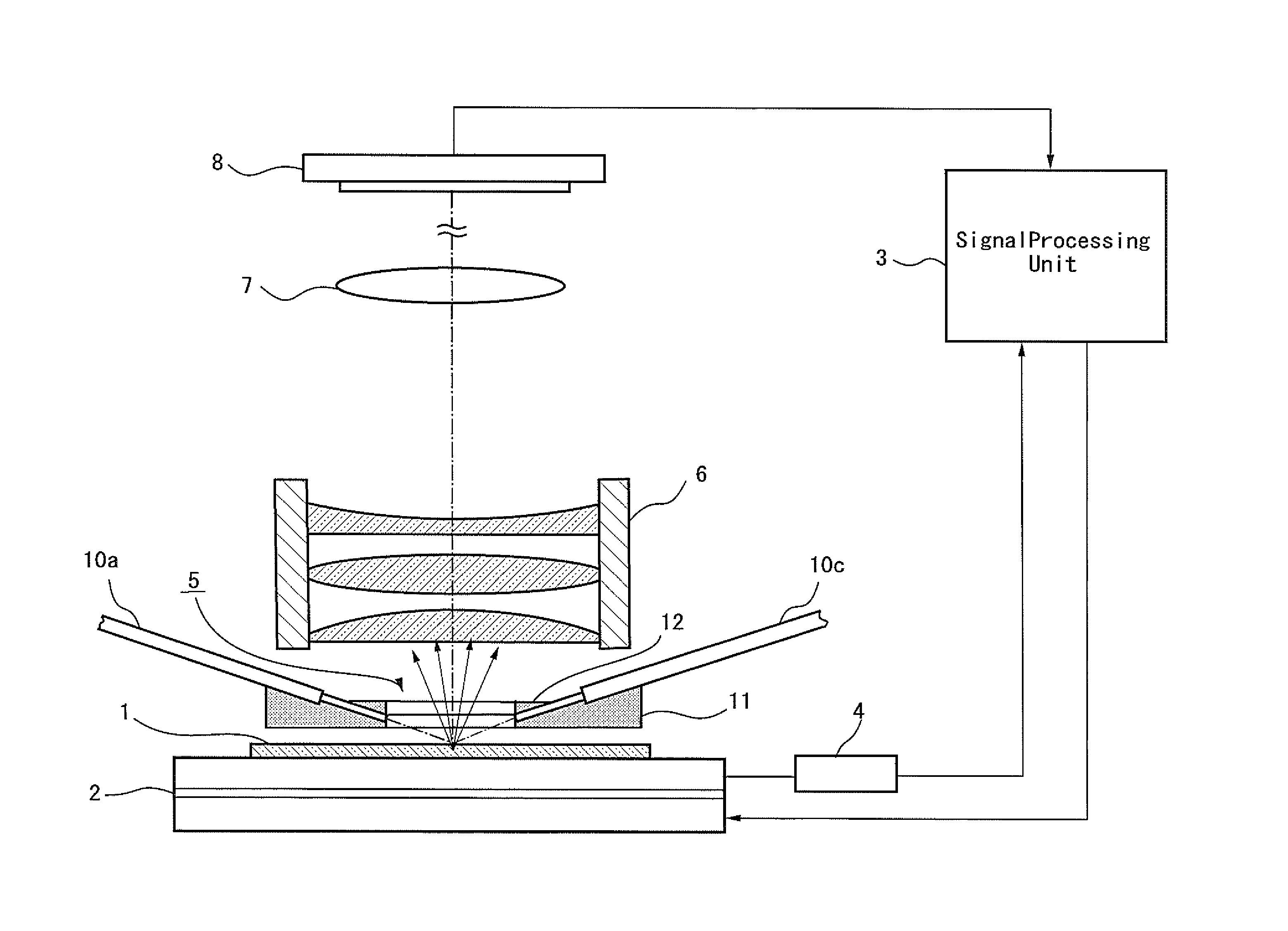
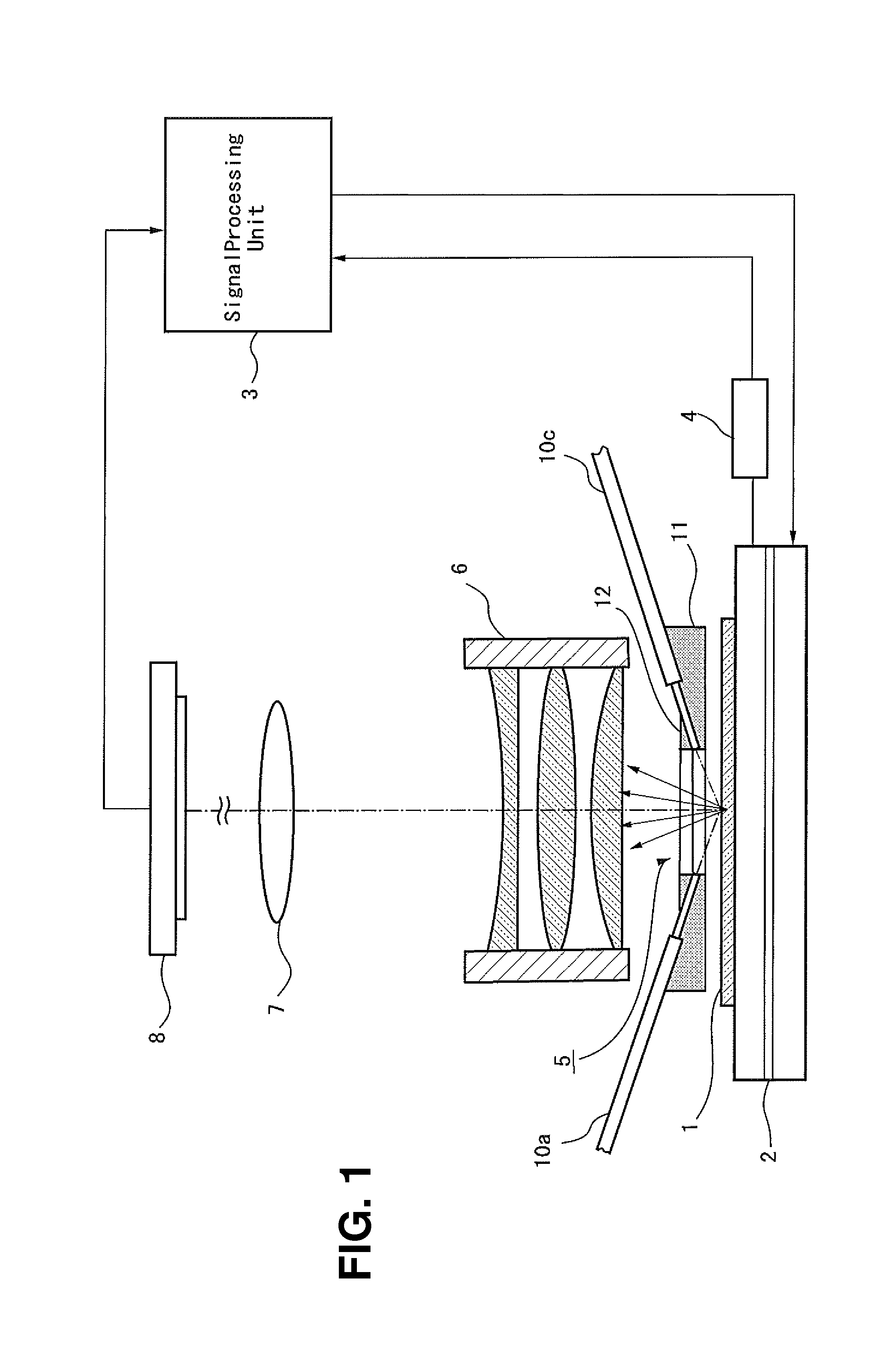
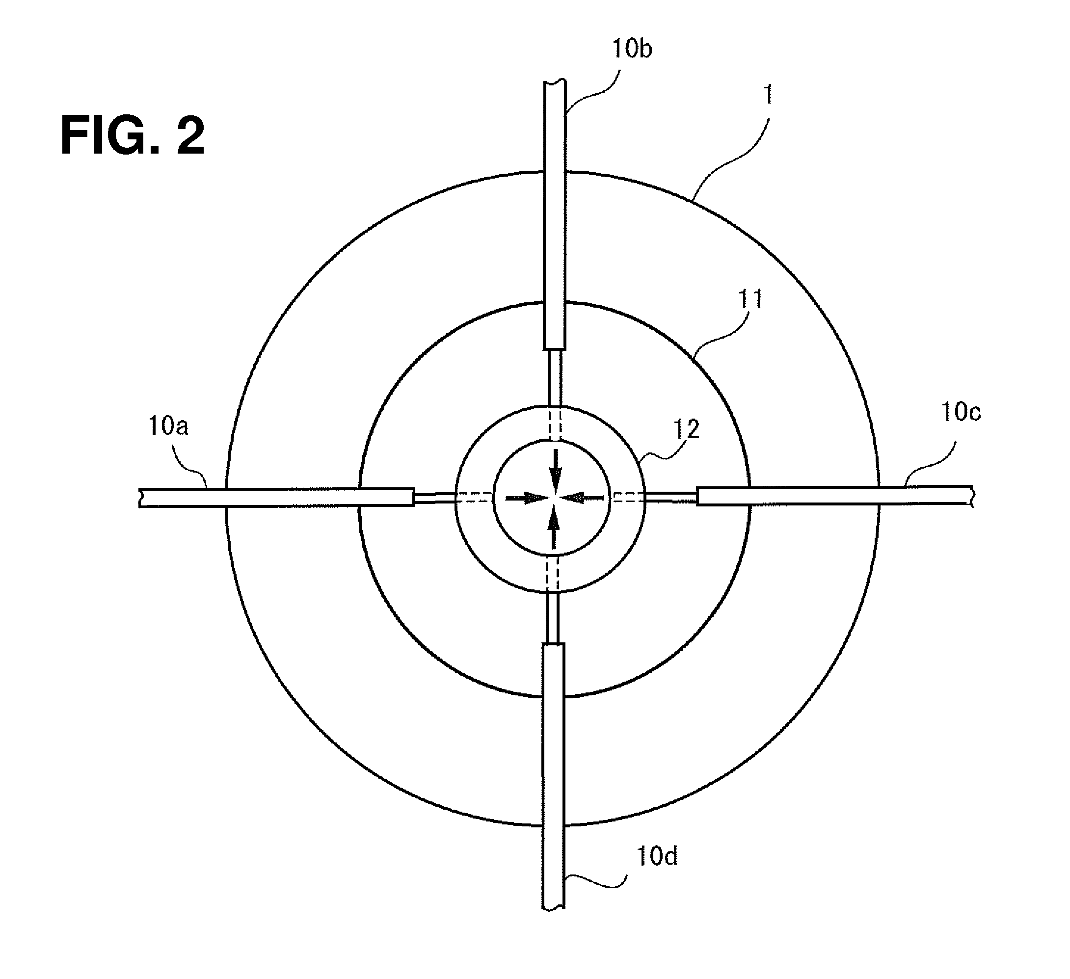
[0059]FIG. 1 is a view showing an overall structure of the inspection apparatus comprising the microscope of the present invention. FIG. 2 is a plan view showing an illumination beam projecting section of the inspection apparatus shown in FIG. 1 and FIG. 3 is a view showing one example of a light source apparatus. According to the invention, the defect detection is carried out by performing dark-field illumination to a sample surface and by detecting scattered light generated in the sample. The sample 1 (semiconductor body) to be inspected is arranged on the stage 2. In the present example, as the substrate to be inspected a semiconductor body comprising a semiconductor substrate and a multilayered structure formed on the substrate is used, and various defects such as a defect formed in the multilayered structure and a defect existing in a wiring pattern are detected. As the semiconductor body, for example a silicon body comprising a silicon substrate and the multilayered structure ...


PUM


Abstract

A system including a microscope and an inspection apparatus in which an objective lens having a large numerical aperture is used for detecting a defect existing inside a sample. A light source apparatus produces linearly polarized light. The polarization maintaining fibers optically coupled to the light source apparatus project the linearly polarized light onto the sample surface as an illumination beam of P-polarized light at an incidence angle substantially equal to the Brewster's angle of the sample. The scattered light generated by the defect existing in the sample is emitted from the sample and is collected by the objective lens whose optical axis is perpendicular to the sample surface. Since the illumination beam of P-polarized light is projected at the incidence angle equal to the Brewster's angle of the sample, no surface reflection occurs and it is possible to use the objective lens having a large numerical aperture.

Description

TECHNICAL FIELD[0001]The present invention relates to a microscope which is suitable to observe and inspect internal structures of various samples from outside of the sample.[0002]The present invention also relates to an inspection apparatus which is suitable to detect a defect existing in a multilayered structure formed on a silicon substrate by use of dark-field illumination.BACKGROUND ART[0003]In a manufacturing process of a semiconductor device, various devices with a trench isolation have been developed. For example, as a MOSFET having high-voltage resistance, a MOSFET having a trench gate structure has been developed. Also, in the manufacturing process of an imaging device such as a CMOS sensor or a CCD sensor, the trenches are formed between the adjacent light receiving elements so as to prevent generation of crosstalk between the pixels. The depth of the trench influences the performance of the device and the yield rate of the production of the devices. For instance, in the ...

Claims


Application Information

Patent Timeline
25 Jul 2013
Publication
US20130188251A1
IPC
G02B21/06
CPC
G02B21/0092; G02B21/10; G02B6/0008; G01N21/9501; G02B21/06; G01N21/9505
Inventors
KUSUNOSE, HARUHIKO; TSUBOUCHI, TAKAO