Coating and developing system with a direct carrying device in a processing block, coating and developing method and storage medium

a technology of developing system and carrying device, applied in the field of coating and developing system, can solve the problems of reducing carrying efficiency, increasing the load on designing and manufacturing, and difficult to improve the throughput of the system, so as to achieve the effect of easy design and manufacturing

Active Publication Date: 2011-08-16
TOKYO ELECTRON LTD
View PDF14 Cites 0 Cited by
  • Summary
  • Abstract
  • Description
  • Claims
  • Application Information

AI Technical Summary

Benefits of technology

[0010]The present invention has been made under such circumstances and it is therefore an object of the present invention to provide techniques facilitating designing and manufacturing a coating and developing system capable of achieving a desired throughput.
[0016]According to the present invention, the processing blocks of the same construction are arranged between the carrier block and the interface block, and the processing rate of the coating and developing system is adjusted by adjusting the number of the processing blocks. Thus a coating and developing system capable of achieving a desired throughput can be easily designed and manufactured

Problems solved by technology

Such construction increases loads on the carrying devices A1 to A5, reduces carrying efficiency and hence it is difficult to improve the throughput of the system.
Therefore, many different types of systems respectively having different numbers of units need to be manufactured according to the demand of users, which increases loads on work for designing and manufacture.
Consequently, load on the transfer arm increases and it is difficult to improve the throughput of the system.
Likewise, it is difficult to reduce loads on work for designing and manufacture.

Method used


Image

  • Coating and developing system with a direct carrying device in a processing block, coating and developing method and storage medium
  • Coating and developing system with a direct carrying device in a processing block, coating and developing method and storage medium
  • Coating and developing system with a direct carrying device in a processing block, coating and developing method and storage medium

Examples


Embodiment Construction

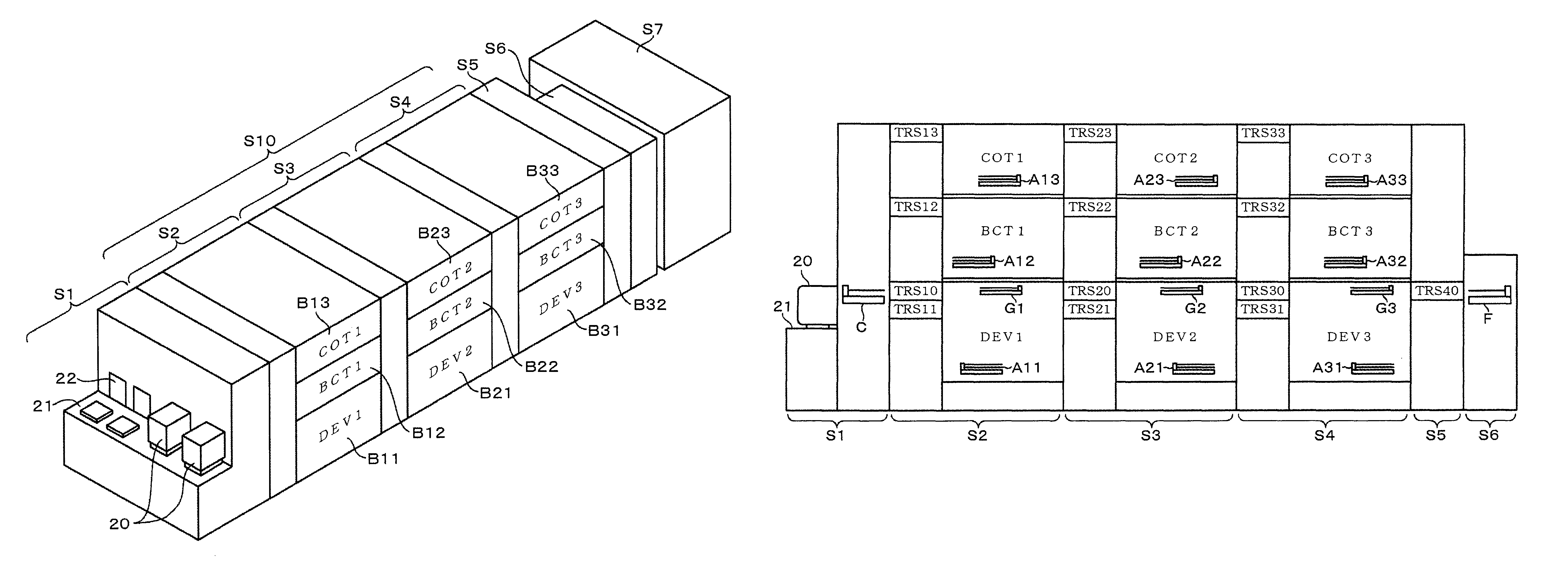
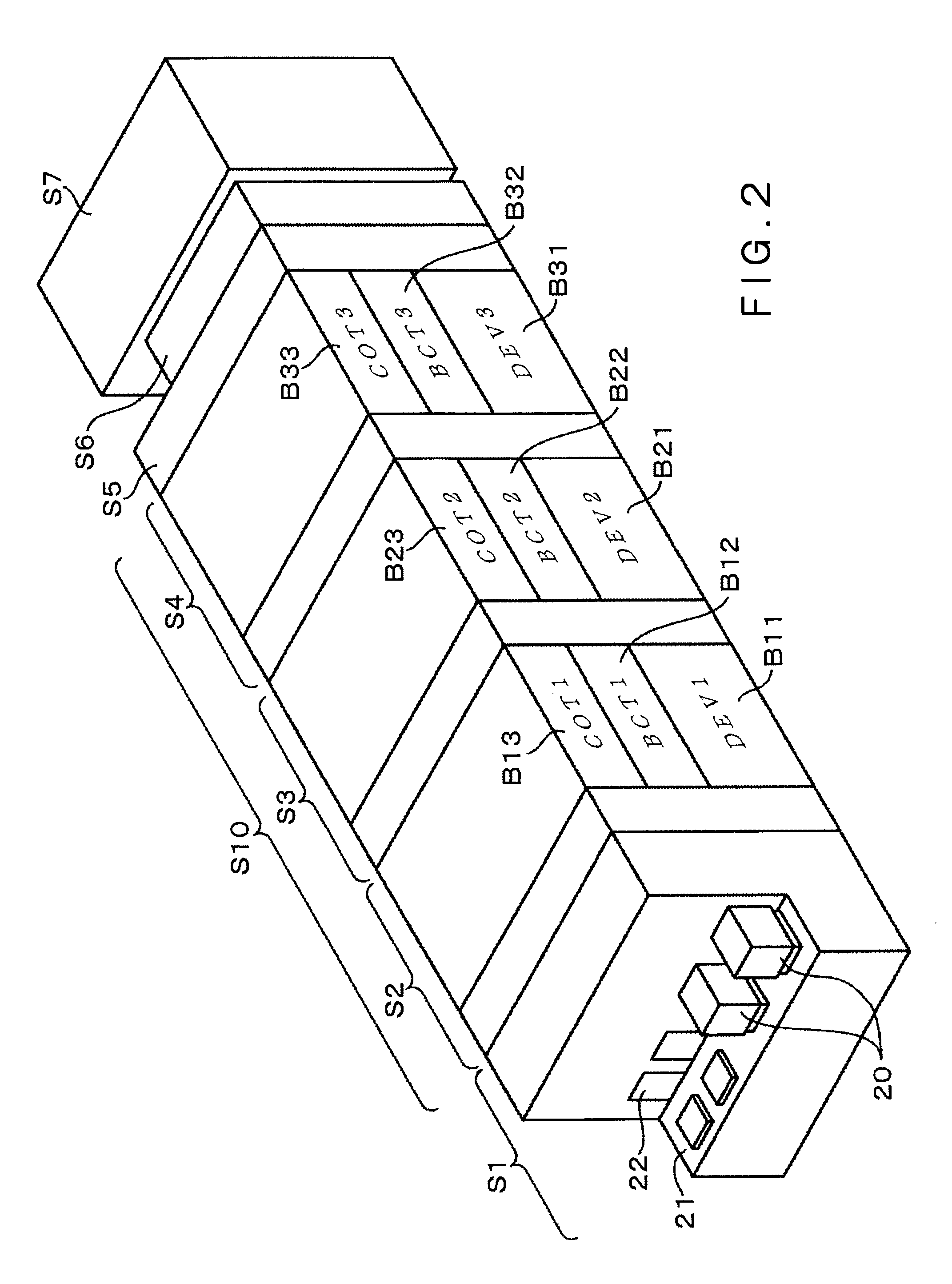
[0027]Resist pattern forming systems in preferred embodiments of a coating and developing system according to the present invention will be described with reference to the accompanying drawings. FIGS. 1, 2 and 3 are a plan view, a schematic perspective view and a schematic side elevation, respectively, of a resist pattern forming system in a first embodiment according to the present invention. The resist pattern forming system has a carrier block S1, a processing station S10, a transfer block S5, an interface block S6, and an exposure system S7. The carrier block S1 is on the front side, and the interface block S6 is on the back side. The carrier block S1, the processing station S10, the transfer block S5, the interface block S6, and the exposure system S7 are arranged longitudinally in that order in a line, and the adjacent ones thereof are connected.

[0028]The carrier block S1 receives and sends out a carrier 20 containing, for example, thirteen wafers W, namely, substrates, in an ...


PUM


Abstract

A coating and developing system includes processing blocks of the same construction each built by stacking up a plurality of unit blocks including a film forming unit block and a developing unit block in layers. The processing blocks are arranged longitudinally between a carrier block and an interface block. The number of processing blocks like the processing blocks arranged between the carrier block and the interface block is adjusted to adjust the throughput of the coating and developing system. Thus, a coating and developing system capable of achieving a desired throughput can be easily designed and manufactured.

Description

BACKGROUND OF THE INVENTION[0001]1. Field of the Invention[0002]The present invention relates to a coating and developing system for coating a substrate, such as a semiconductor wafer or an LCD substrate, namely, a glass substrate for a liquid crystal display, with a resist solution by a coating process and processing the substrate by a developing process after exposure, a coating and developing method to be carried out by the coating and developing system, and a storage medium.[0003]2. Description of the Related Art[0004]A manufacturing process for manufacturing a semiconductor device or an LCD substrate forms a resist patter on a substrate by photolithography. Photolithography includes a series of steps of coating a surface of a substrate, such as a semiconductor wafer (hereinafter, referred to as “wafer”) with a resist film by applying a resist solution to the surface, exposing the resist film to light through a photomask, and processing the exposed resist film by a developing pr...

Claims


Application Information

Patent Timeline
Patent Type & Authority Patents(United States)
IPC IPC(8): G03D5/04
CPCH01L21/67745H01L21/67178G05B19/4189G05B2219/31002H01L21/67196H01L21/67742
Inventor MATSUOKA, NOBUAKIHASHIMOTO, TAKAHIROTSUCHIYA, KATSUHIROHAYASHI, SHINICHIHAYASHIDA, YASUSHI
Owner TOKYO ELECTRON LTD
Why Eureka
Try Eureka