Image sensor and manufacturing method thereof

a technology of image sensor and manufacturing method, which is applied in the direction of electrical equipment, semiconductor devices, radio frequency controlled devices, etc., can solve the problems of reducing the fill factor and limiting the possibility of resolution

Inactive Publication Date: 2011-09-20
DONGBU HITEK CO LTD
View PDF7 Cites 165 Cited by
  • Summary
  • Abstract
  • Description
  • Claims
  • Application Information

AI Technical Summary

Problems solved by technology

Accordingly, an additional region for a photodiode is required on the substrate for each unit pixel, which reduces a fill factor and limits possibility of resolution.

Method used


Image

  • Image sensor and manufacturing method thereof
  • Image sensor and manufacturing method thereof
  • Image sensor and manufacturing method thereof

Examples


Embodiment Construction

[0010]Embodiments of an image sensor and a manufacturing method thereof are described in detail with reference to the accompanying drawings.

[0011]When the terms “on” or “over” are used herein, when referring to layers, regions, patterns, or structures, it is understood that the layer, region, pattern or structure can be directly on another layer or structure, or intervening layers, regions, patterns, or structures may also be present. When the terms “under” or “below” are used herein, when referring to layers, regions, patterns, or structures, it is understood that the layer, region, pattern or structure can be directly under the other layer or structure, or intervening layers, regions, patterns, or structures may also be present.

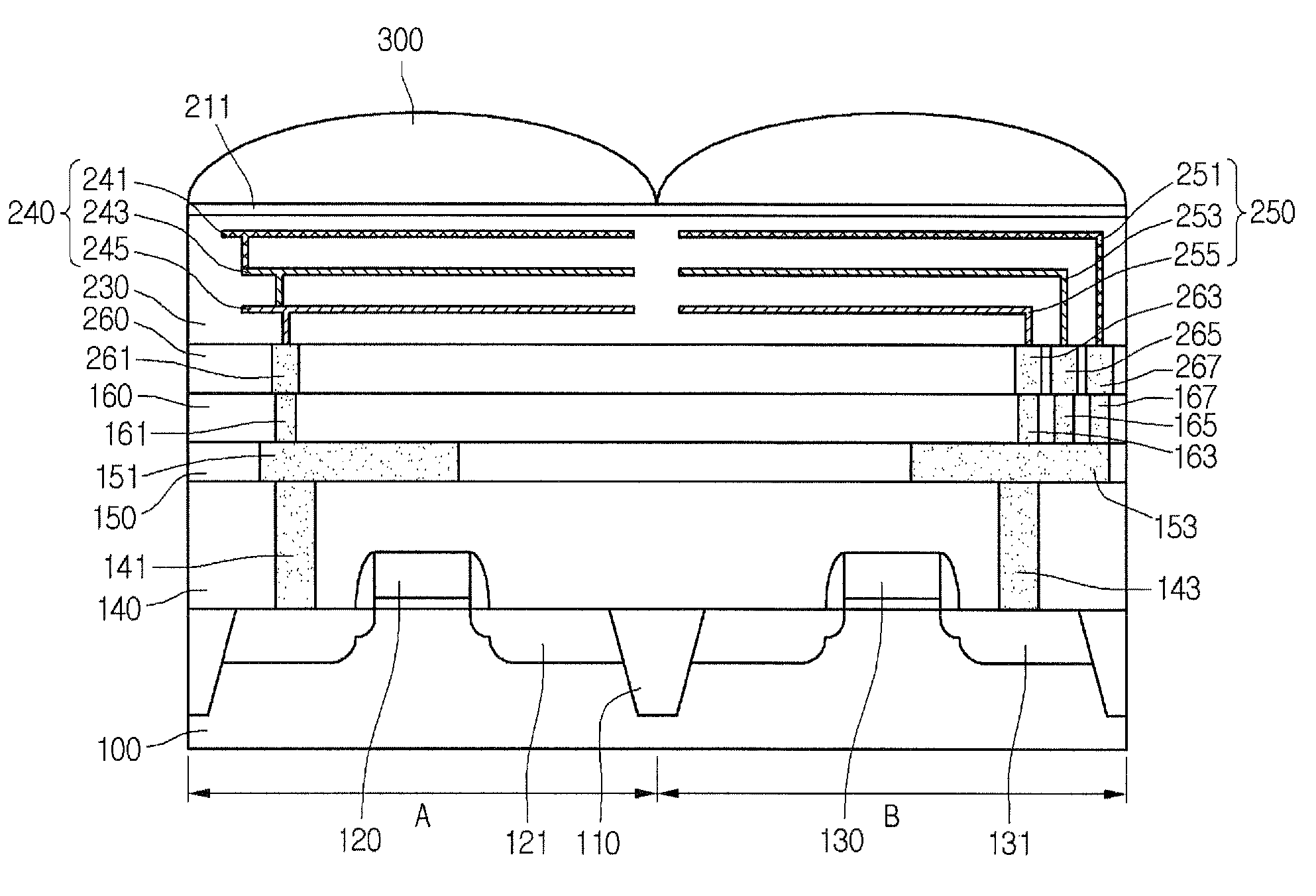
[0012]FIG. 9 is a cross-sectional view of an image sensor according to an embodiment.

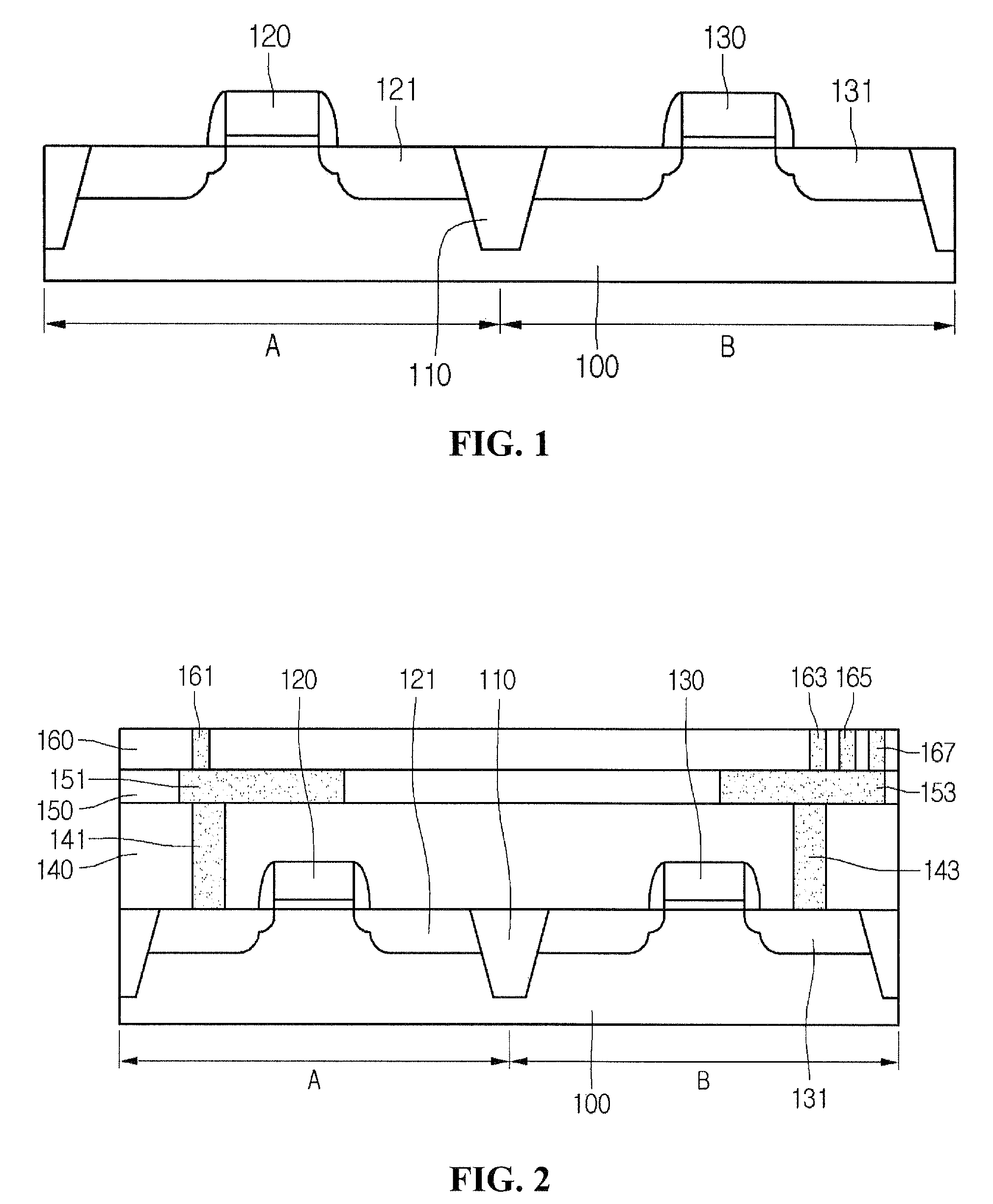
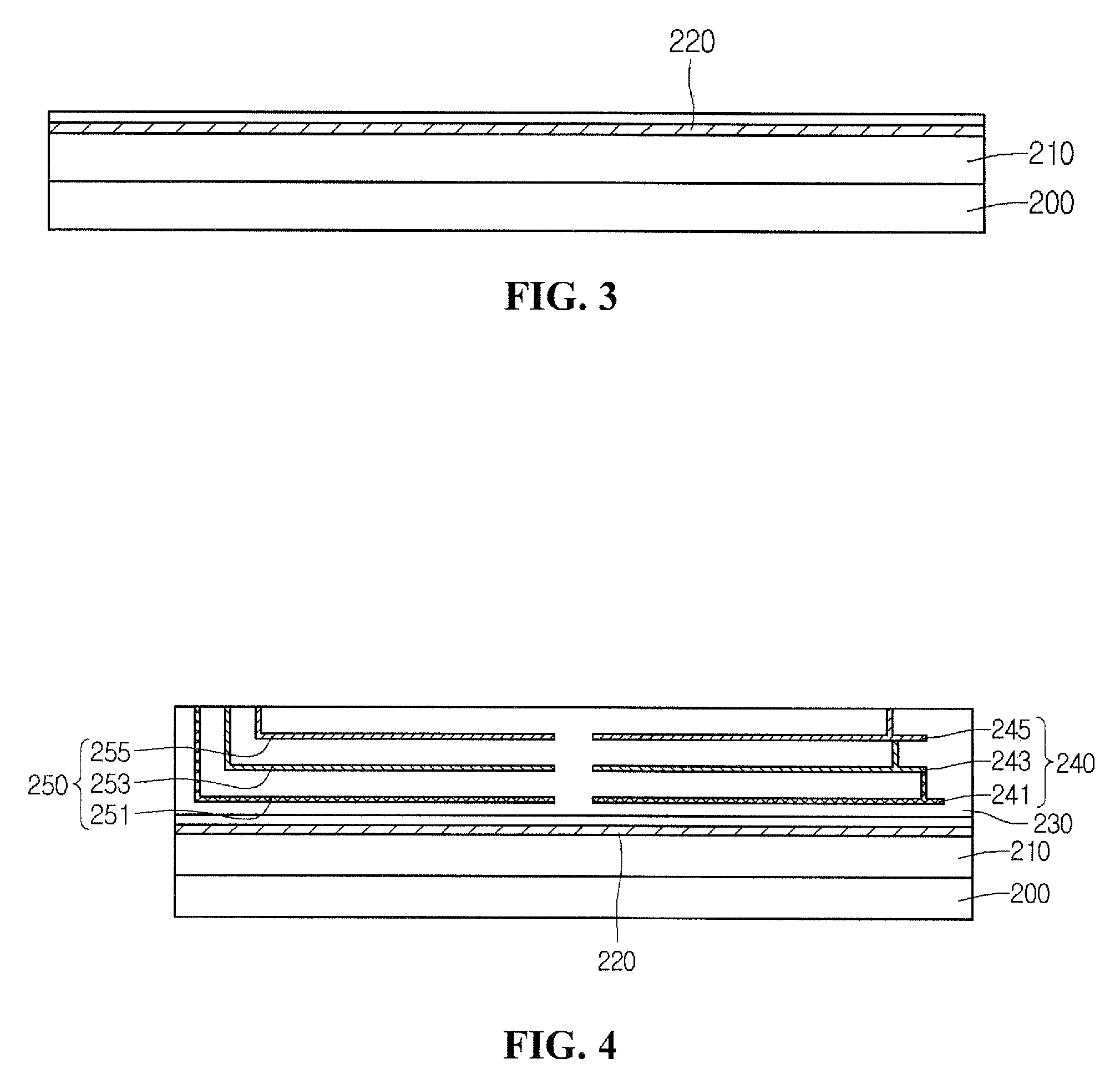
[0013]Referring to FIG. 9, a second substrate 211 including photodiodes 240 and 250 can be disposed on a first substrate 100 including transistors 120 and 130 respectively ...


PUM


Abstract

Provided are embodiments of an image sensor. The image sensor can comprise a first substrate including a transistor circuit, a lower interconnection layer, an upper interconnection layer, and a second substrate including a vertical stacked photodiode. The lower interconnection layer is disposed on the first substrate and comprises a lower interconnection connected to the transistor circuit. The upper interconnection layer is disposed on the lower interconnection layer and comprises an upper interconnection connected with the lower interconnection. The vertical stacked photodiode can be disposed on the upper interconnection layer and connected with the upper interconnection through, for example, a single plug connecting a blue, green, and red photodiode of the vertical stack or a corresponding plug for each of the blue, green, and red photodiode of the vertical stack.

Description

CROSS-REFERENCE TO RELATED APPLICATION[0001]The present application claims the benefit under 35 U.S.C. §119 of Korean Patent Application No. 10-2007-0097281, filed Sep. 27, 2007, which is hereby incorporated by reference in its entirety.BACKGROUND[0002]An image sensor is a semiconductor device for converting an optical image into an electrical signal. The image sensor is roughly classified as a charge coupled device (CCD) image sensor or a complementary metal oxide semiconductor (CMOS) image sensor (CIS).[0003]The CIS includes photodiodes and MOS transistors in a unit pixel, and sequentially detects electrical signals of respective unit pixels in a switching manner to realize an image. Particularly, the unit pixel of a typical CIS includes a photodiode region receiving a light signal to convert the light signal into an electrical signal and a transistor region processing this electrical signal.[0004]In a horizontal CMOS image sensor, the photodiode and the transistor are horizontall...

Claims


Application Information

Patent Timeline
Patent Type & Authority Patents(United States)
IPC IPC(8): H01L31/00H01L27/146
CPCH01L27/14632H01L27/14634H01L27/14636H01L27/1469
Inventor BANG, SUN KYUNG
Owner DONGBU HITEK CO LTD
Why Eureka
Try Eureka