

Semiconductor device, manufacturing method and transistor circuit
A technology of transistors and semiconductors, which is applied in semiconductor devices, semiconductor/solid-state device components, electric solid-state devices, etc., can solve the problems of thin insulating layers that are easily damaged, and the withstand voltage of GaN-HEMT is not high, so as to improve the withstand voltage Effect
- Summary
- Abstract
- Description
- Claims
- Application Information
AI Technical Summary
Problems solved by technology
Method used
Image

Examples
no. 1 Embodiment
[0037] (1) Structure
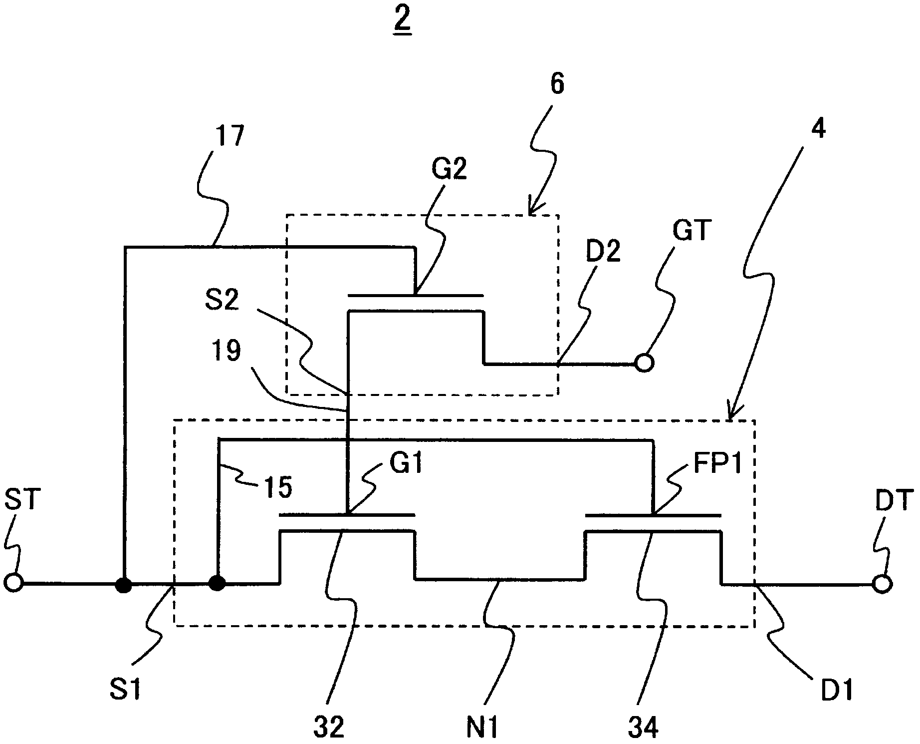
[0038] figure 1 is a circuit diagram of the transistor circuit 2 according to the present embodiment. The transistor circuit 2 comprises a first high electron mobility transistor 4 and a second high electron mobility transistor 6 with a negative threshold voltage. exist figure 1 The equivalent circuits of the first high-electron-mobility transistor 4 and the second high-electron-mobility transistor 6 are shown in boxes drawn with dotted lines in .
[0039] Such as figure 1 As shown, the second source S2 of the second high electron mobility transistor 6 is coupled to the first gate G1 of the first high electron mobility transistor 4 . Moreover, the second gate G2 of the second high electron mobility transistor 6 is coupled to the first source S1 of the first high electron mobility transistor 4 .
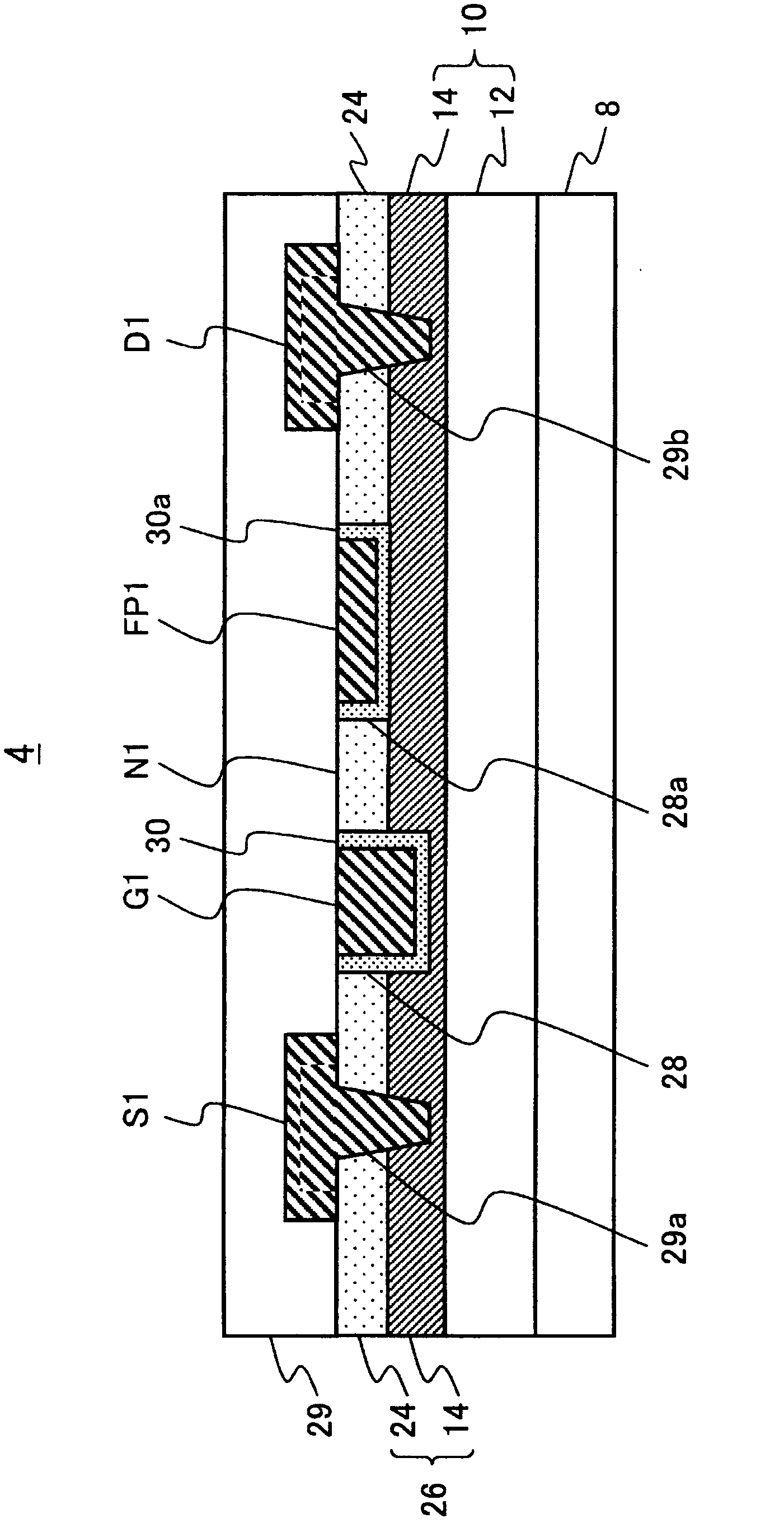
[0040] figure 2 is the cross section of the first high electron mobility transistor 4 . Such as figure 2 As shown, the first high electron mobility tr...
no. 2 Embodiment
[0119] Image 6 is a plan view of the transistor circuit 2b according to the present embodiment. In the first embodiment, a first high electron mobility transistor 4 is coupled to a second high electron mobility transistor 6 . On the other hand, if Image 6 As shown, in the transistor circuit 2 b according to this embodiment, a plurality of first high electron mobility transistors 4 are coupled to one second high electron mobility transistor 6 . Here, the first high electron mobility transistor 4 and the second high electron mobility transistor 6 are devices formed on the same substrate.
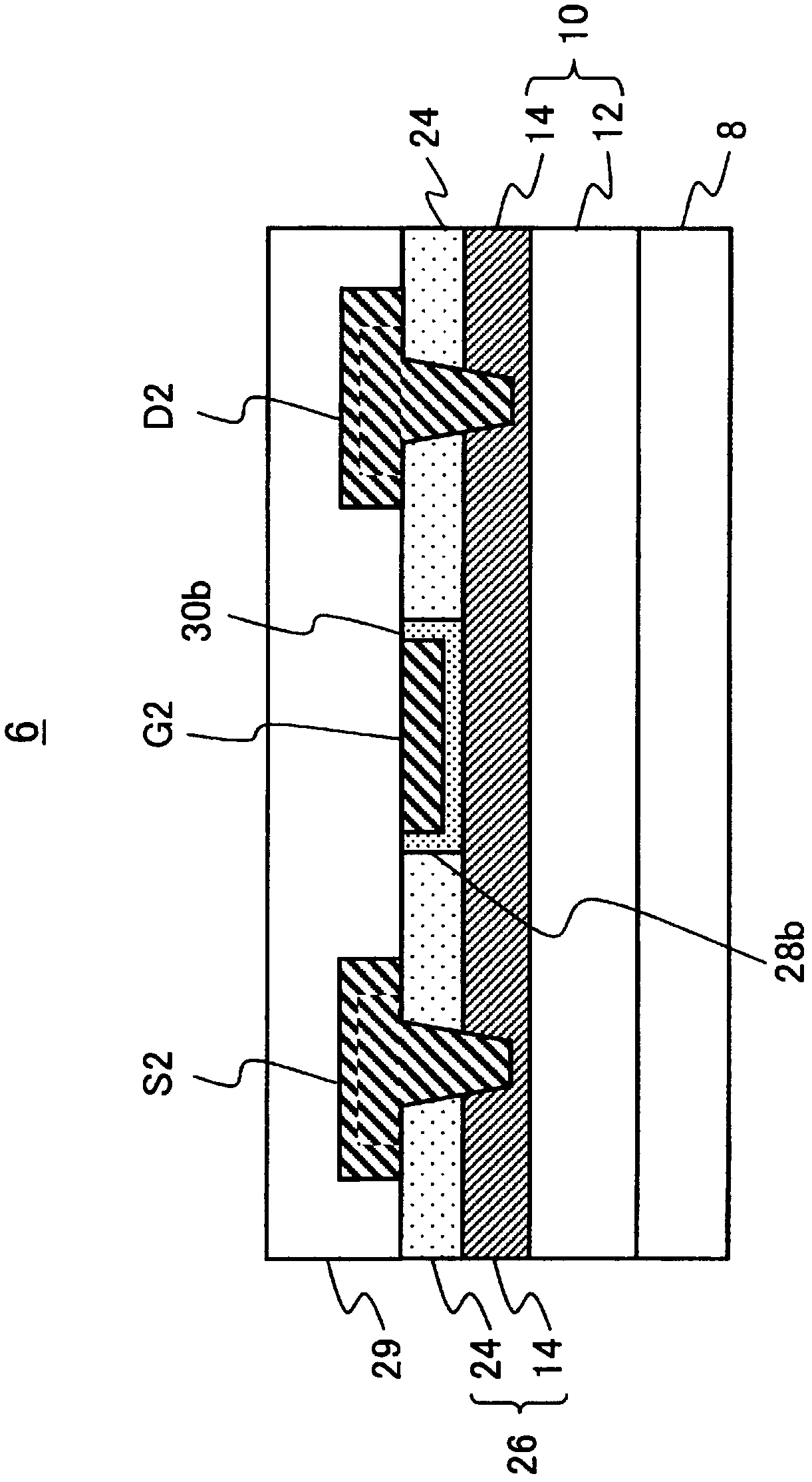
[0120] The structures of the first high electron mobility transistor 4 and the second high electron mobility transistor 6 are the same as those according to the first embodiment (refer to figure 2 , image 3 The structures of the first high electron mobility transistor and the second high electron mobility transistor described above are substantially the same. For example, a region bet...
no. 3 Embodiment
[0130] Figure 8 is a circuit diagram of the transistor circuit 2d according to the present embodiment. Such as Figure 8 As shown, the transistor circuit 2d is similar to the transistor circuit 2 of the first embodiment. Therefore, descriptions of parts common to the transistor circuit 2 of the first embodiment will be omitted.
[0131] Such as Figure 8 As shown, the transistor circuit 2d includes a first high electron mobility transistor 4a and a second high electron mobility transistor 6a.
[0132] (1) The first high electron mobility transistor
[0133] The first high electron mobility transistor 4 a includes a first gate G1 , a first field plate FP1 a and a second field plate FP2 .
[0134] Similar to the first field plate FP1 in the first embodiment, the first field plate FP1a is a field plate provided between the first gate G1 and the first drain D1. The first field plate FP1a may be a field plate of which a portion extends between the first gate G1 and the first...
PUM
 Abstract
Description
Claims
Application Information