Sustain driver, sustain control system, and plasma display

a control system and driver technology, applied in the field of sustain driver, can solve the problems of destroying the mosfet, spoiling the reliability of the output circuit, and increasing the risk of simultaneous turning-on of the two power mosfets, so as to improve the reliability of the overvoltage protection circuit and improve the integration and high reliability

Inactive Publication Date: 2005-06-23
COLLABO INNOVATIONS INC
View PDF6 Cites 37 Cited by
  • Summary
  • Abstract
  • Description
  • Claims
  • Application Information

AI Technical Summary

Benefits of technology

[0016] An object of the present invention is to provide a control circuit of a sustain driver that can achieve further improvements both in high integration and high reliability, by further improving the reliability of the overvoltage protection circuit with its area maintained small.
[0057] The n type epitaxial layer, the second n type diffusion region, and the first n type diffusion region is used as collector, emitter, and base regions of the bipolar transistor circuit, respectively. As described above, the base current is maintained much smaller than the collector current. Accordingly, the first p and n type diffusion regions may be rather smaller than the other diffusion regions. Thus, the bipolar transistor circuit according to the invention is easy to miniaturize with high reliability maintained.
[0060] In the above-described control circuit according to the invention, further preferably, the level shift circuit comprises a reverse current blocking diode inserted between the high side power supply terminal and the level shift transistor and cutting off the current flowing in the direction from the level shift transistor to the high side power supply terminal. When the potential of the high side power supply terminal falls below the potential of the input terminal of the high side circuit, the reverse current blocking diode prevents the reverse current from flowing from the level shift transistor to the high side power supply terminal. Thereby, the occurrence of the excessive voltage drop across the resistance element due to the reverse current is avoided. Thus, the high side circuit is protected from the transient overvoltage as well. Accordingly, the above-described control circuit according to the invention can maintain further high reliability.
[0061] When the control circuit according to the invention is configured as the above-described integrated circuit on the substrate, preferably, the reverse current blocking diode includes: a third p type diffusion region formed within the n type epitaxial layer and connected to the high side power supply terminal; and a third n type diffusion region formed within the third p type diffusion region and connected to the input terminal of the high side circuit. In this control circuit, the reverse current blocking diode and the resistance element are arranged within the above-described n type epitaxial layer, together with the above-described bipolar transistor circuit, and separated from the outside by the above-described p type separation region. As a result, the above-described control circuit according to the invention has a further higher packing density.
[0062] In the control circuit of the sustain driver according to the invention, as described above, the bipolar transistor circuit is used for the overvoltage protection of the high side circuit. Thereby, the reliability of the overvoltage protection circuit further improves with its area maintained small. In other words, the control circuit according to the invention can further improve both in high integration and high reliability, in contrast to the conventional circuit.
[0063] The improvement in high reliability of the control circuit greatly contributes to the improvement in high reliability of the output circuit, and in particular, effectively prevents the destruction of the output transistor due to the shoot-through current. On the other hand, the further higher integration of the control circuit further reduces its chip size. As a result, the manufactures' costs of the sustain driver, and further of the plasma display, can be reduced.

Problems solved by technology

Furthermore, the MOSFETs may be at the risk of destruction.
In addition, the malfunction of the high side circuit 5H leads the malfunction of the output circuit 20, and thus, spoils the reliability of the output circuit 20, and furthermore, increases the risk of the simultaneous turn-on of the two power MOSFET 2H and 2L.
As a result, further miniaturization of the sustain driver and its resulting further reduction of the manufactures' costs are difficult.

Method used


Image

  • Sustain driver, sustain control system, and plasma display
  • Sustain driver, sustain control system, and plasma display
  • Sustain driver, sustain control system, and plasma display

Examples


embodiment 1

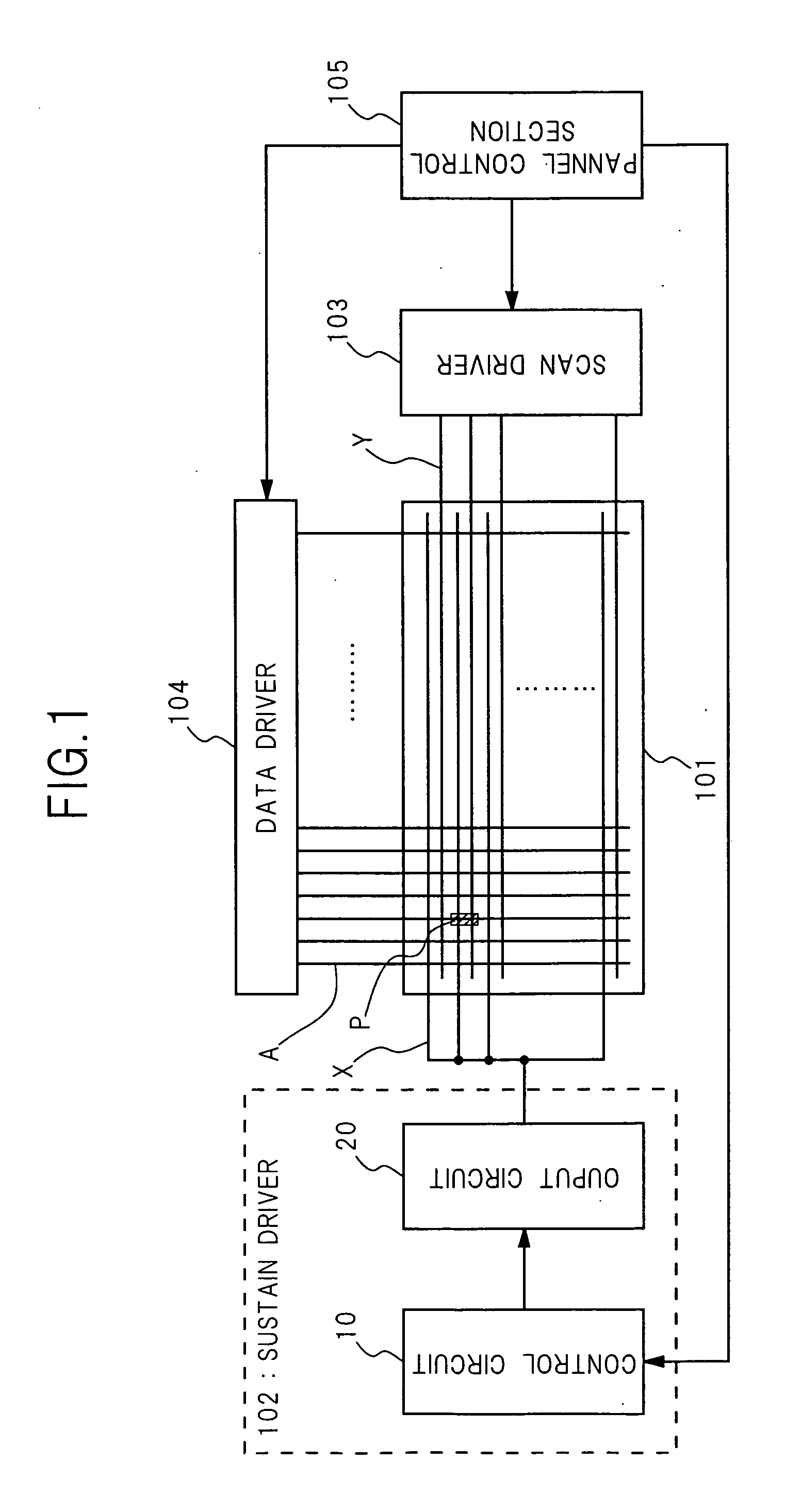
[0075] A plasma display according to Embodiment 1 of the present invention comprises a PDP 101, a sustain driver 102, a scan driver 103, a data driver 104, and a panel control section 105. See FIG. 1.

[0076] The PDP 101 is preferably an AC type and comprises a three-electrode surface-discharge type structure. Three by n (n: integer) address electrodes A are arranged on the rear substrate of the PDP 101 in the vertical direction of the panel. m (m: integer) sustain electrodes X and m scan electrodes Y are alternately arranged on the front substrate of the PDP 101 in the horizontal direction of the panel. The sustain electrodes X are connected to each other and accordingly, maintained at substantially equal potentials. As for the address and scan electrodes Y, each electrode allows an individual potential change. A discharge cell P is installed at the intersection of the adjacent pair of the sustain electrode X and the scan electrode Y and the address electrode A. Gas fills the inside...

embodiment 2

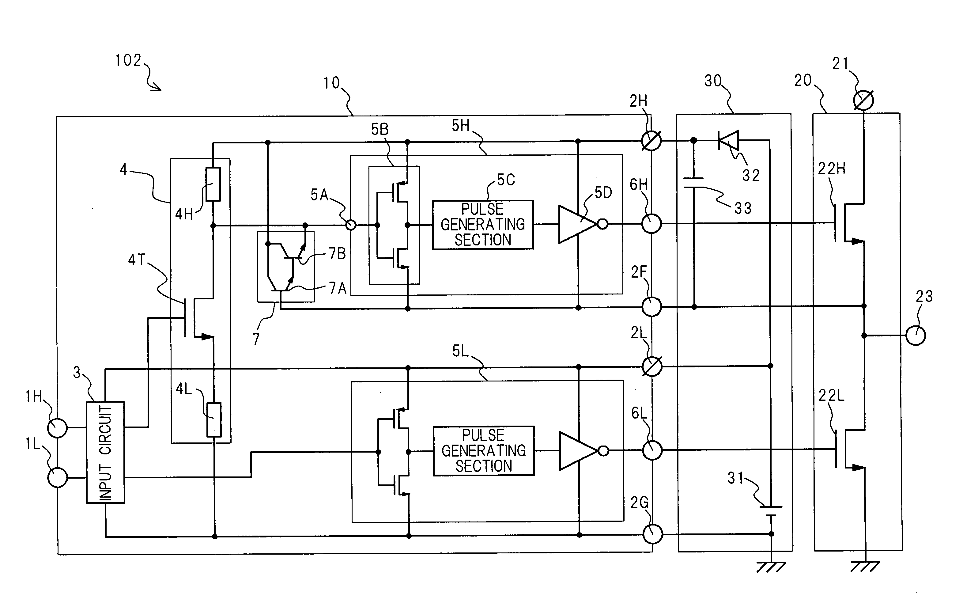
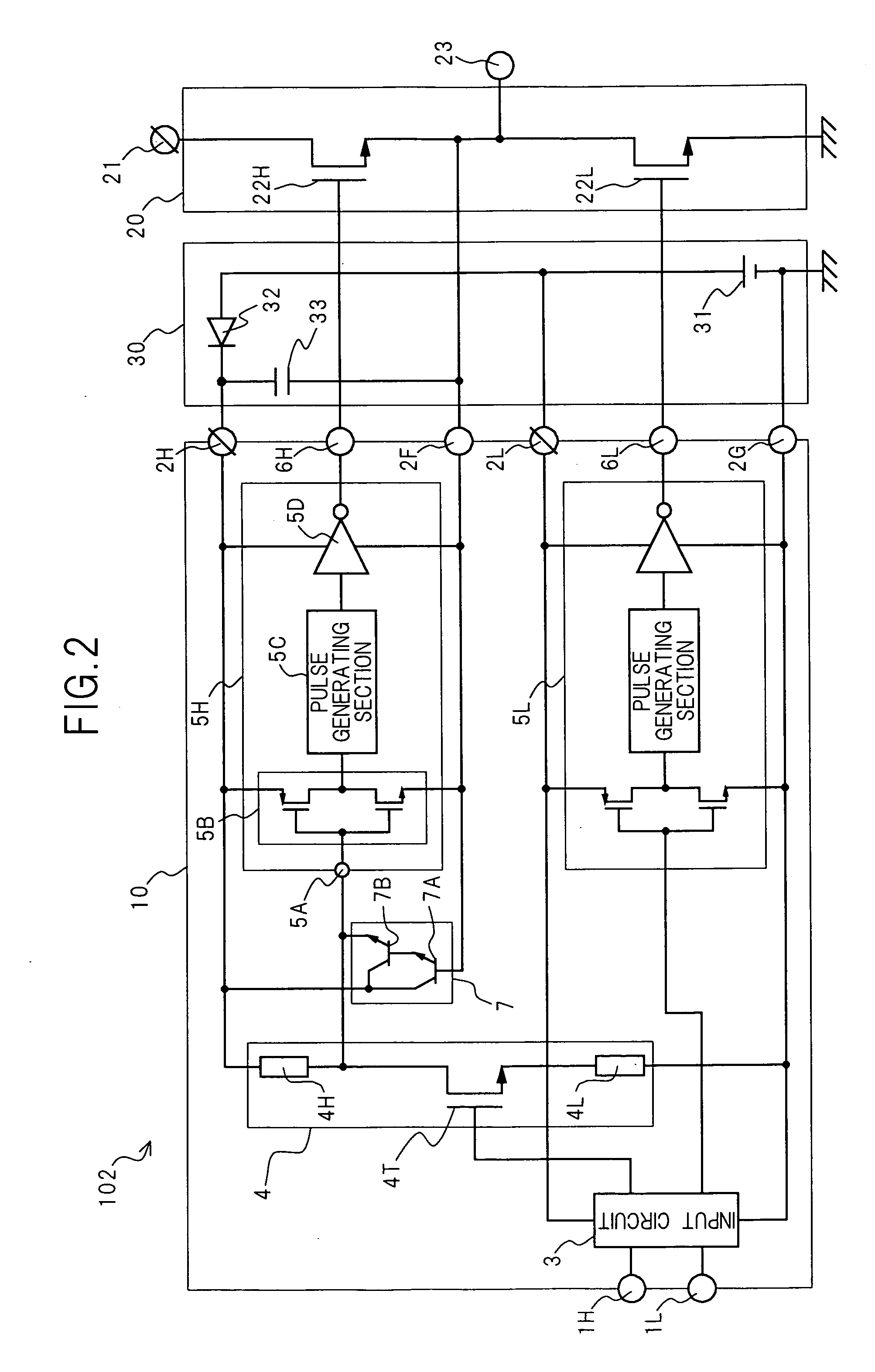
[0112] A control circuit 10 of the sustain driver according to Embodiment 2 of the invention (cf. FIG. 5) comprises circuitry similar to that of the control circuit 10 according to Embodiment 1 of the invention (cf. FIG. 2). However, in the control circuit 10 according to Embodiment 2 of the invention, the level shift circuit 4 further includes a reverse current blocking diode 4B, in contrast to the control circuit 10 according to Embodiment 1 of the invention. In FIG. 5, the components similar to the components shown in FIG. 2 are marked with the same reference symbols as the reference symbols shown in FIG. 2. Furthermore, as for the details of those similar components, an explanation about Embodiment 1 is cited.

[0113] The reverse current blocking diode 4B is, preferably, inserted between the pull-up resistance element 4H and the drain of the level shift transistor 4T. The anode of the reverse current blocking diode 4B is connected to the pull-up resistance element 4H, while the c...


PUM


Abstract

The collector, emitter, and base of a bipolar transistor circuit are connected to a high side power supply terminal, the drain of a level shift transistor, and a floating power supply terminal, respectively. When a high side output transistor is on, the floating power supply terminal is at the potential of a high potential power supply terminal. The high side power supply terminal is at a potential higher than the potential of the floating power supply terminal by a constant voltage. Turning the level shift transistor on, its drain potential drops below the potential of the floating power supply terminal; The base current flows through the bipolar transistor circuit and the drain potential of the level shift transistor is clamped near the potential of the floating power supply terminal; The bipolar transistor circuit is turned on and its collector current supplies the drain current of the level shift transistor.

Description

BACKGROUND OF THE INVENTION [0001] This invention relates to a sustain driver that applies a sustaining voltage pulse to the electrodes of a plasma display panel (PDP), and in particular, relates to the control circuit for the sustain driver. [0002] Plasma displays are display devices of the self-emission type, which use a light emission phenomenon caused by a discharge in gas. Plasma display panels (PDPs) are easy to upsize and slim down in contrast to other display devices, and furthermore, have advantages in flicker-free images, high contrasts, high-speed responses, and so on. Because of these advantages, plasma displays have become widespread in recent years, which are served as next-generation image display devices in place of CRTs (cathode-ray tubes). [0003] A PDP comprises a basic structure with two substrates laminated. For example, in the structure of an AC type PDP, or in particular, the three-electrode surface-discharge type structure, a plurality of address electrodes ar...

Claims


Application Information

Patent Timeline
Patent Type & Authority Applications(United States)
IPC IPC(8): G09G3/20G09G3/291G09G3/294G09G3/296H01L21/822H01L21/8238H01L27/04H01L27/06H01L27/092H03K17/687
CPCG09G3/282G09G3/288G09G3/294G09G2330/04G09G2300/0408G09G2310/0289G09G3/296
Inventor SASADA, MASAHIKOMATSUNAGA, HIROKIINAO, MASASHIANDO, HIROSHIKANEDA, JINSAKUMAEDA, EISAKUMAEJIMA, AKIHIRO
Owner COLLABO INNOVATIONS INC
Why Eureka
Try Eureka