Circuits providing ESD protection to high voltage laterally diffused metal oxide semiconductor (LDMOS) transistors

a metal oxide semiconductor and transistor technology, applied in semiconductor devices, semiconductor/solid-state device details, diodes, etc., can solve problems such as contact spiking, silicon melting, or metal interconnect melting, and integrated circuit devices are susceptible to damage from excessive voltage application,

Active Publication Date: 2010-11-23
MONTEREY RES LLC
View PDF51 Cites 35 Cited by
  • Summary
  • Abstract
  • Description
  • Claims
  • Application Information

AI Technical Summary

Benefits of technology

[0009]The problems outlined above may be in large part addressed by a circuit providing ESD protection to high voltage laterally diffused metal oxide semiconductor (LDMOS) transistors. The following are mere exemplary embodiments of the circuit and are not to be construed in any way to limit the subject matter of the claims.

Problems solved by technology

As is well known in the microelectronics industry, integrated circuit devices are susceptible to damage from application of excessive voltages, such as, for example, electrostatic discharge (ESD) events.
In particular, during an ESD event, charge transferred within a circuit can develop voltages that are large enough to break down insulating films (e.g., gate oxides) on the device or dissipate sufficient energy to cause electrothermal failures in the device.
Such failures include contact spiking, silicon melting, or metal interconnect melting.
In developing effective ESD protection circuitry, circuit designers may, however, be limited with regard to the particular structures used, since the protection circuit must integrate well with the remainder of the integrated circuit.
Although DEMOS transistors are effective for operations at high voltage levels, DEMOS transistors are inherently susceptible to damage from ESD events due to their device structure.
Such a configuration, however, relies on drain breakdown of the active DEMOS transistor to trigger the SCR.
In some cases, triggering the SCR in such a manner may not be fast enough to prevent the active DEMOS transistor from being damaged and, therefore, may not be effective for many applications.
In general, however, such configurations have limited controllability of the trigger and holding voltages of the SCR.
As a consequence, the level of ESD protection offered by such prior art designs is limited.

Method used


Image

  • Circuits providing ESD protection to high voltage laterally diffused metal oxide semiconductor (LDMOS) transistors
  • Circuits providing ESD protection to high voltage laterally diffused metal oxide semiconductor (LDMOS) transistors
  • Circuits providing ESD protection to high voltage laterally diffused metal oxide semiconductor (LDMOS) transistors

Examples


Embodiment Construction

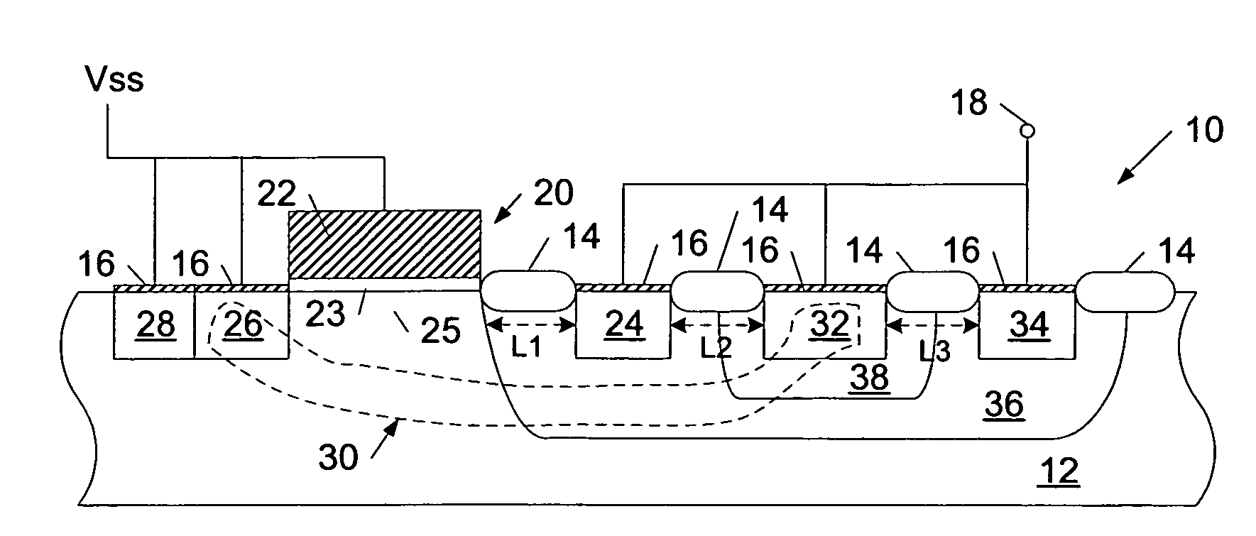
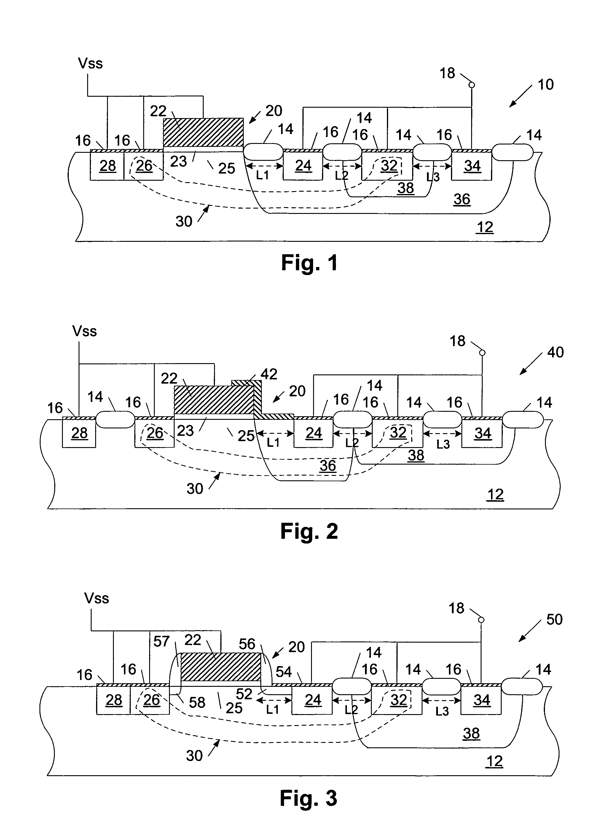
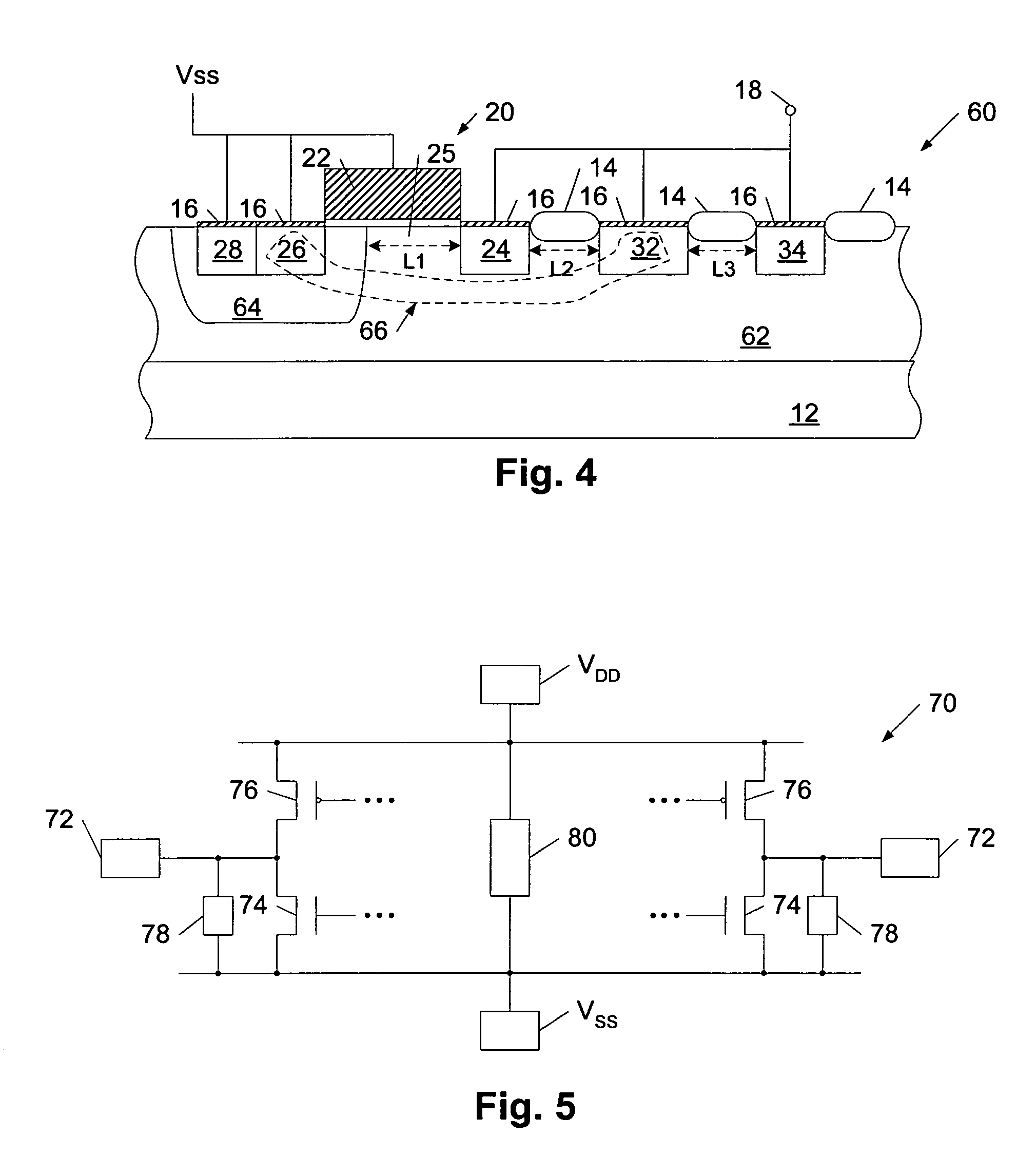
[0020]Turning to the drawings, exemplary devices for protecting laterally diffused metal oxide semiconductor (LDMOS) output driver transistors from damage caused by electrostatic discharge (ESD) events are illustrated in FIGS. 1-4. More specifically, cross-sectional views of exemplary semiconductor topographies, which are configured to divert charge from a bus coupled to an active LDMOS output driver transistor (i.e., a LDMOS pull-down output driver transistor or a LDMOS pull-up output driver transistor), are shown in FIGS. 1-4. In addition, FIG. 5 illustrates a schematic of an exemplary circuit detailing an arrangement of one or more of the semiconductor topographies depicted in FIGS. 1-4 in positions relative to output driver transistors, signal pads, and power supply pads of the circuit. As discussed in reference to FIG. 5, the ESD protection devices described herein are distinct from the active LDMOS output driver transistors they are used to protect and, as such, the protection...


PUM


Abstract

Circuits including a laterally diffused output driver transistor and a distinct device configured to provide electrostatic discharge (ESD) protection for the laterally diffused output driver transistor are presented. In general, the device configured to provide ESD protection includes a drain extended metal oxide semiconductor transistor (DEMOS) transistor configured to breakdown at a lower voltage than a breakdown voltage of the laterally diffused output driver transistor. The laterally diffused output driver transistor may be a pull-down or a pull-up output driver transistor. The device also includes a silicon controlled rectifier (SCR) configured to inject charge within a semiconductor layer of the circuit upon breakdown of the DEMOS transistor. Moreover, the device includes a region configured to collect the charge injected from the SCR and further includes an ohmic contact region configured to at least partially affect the holding voltage of the SCR.

Description

BACKGROUND OF THE INVENTION[0001]1. Field of the Invention[0002]The present invention relates generally to devices and circuits providing electrostatic discharge (ESD) protection, and more particularly, to devices and circuits providing ESD protection to high voltage laterally diffused metal oxide semiconductor (LDMOS) transistors.[0003]2. Description of the Related Art[0004]The following descriptions and examples are given as background information only.[0005]As is well known in the microelectronics industry, integrated circuit devices are susceptible to damage from application of excessive voltages, such as, for example, electrostatic discharge (ESD) events. In particular, during an ESD event, charge transferred within a circuit can develop voltages that are large enough to break down insulating films (e.g., gate oxides) on the device or dissipate sufficient energy to cause electrothermal failures in the device. Such failures include contact spiking, silicon melting, or metal inte...

Claims


Application Information

Patent Timeline
Patent Type & Authority Patents(United States)
IPC IPC(8): H01L23/62
CPCH01L27/0262H01L27/0266H01L29/87
Inventor WALKER, ANDREW J.PUCHNER, HELMUTKUTZ, HAROLD M.SHUTT, JAMES H.
Owner MONTEREY RES LLC
Why Eureka
Try Eureka