Method of manufacturing microlens

a manufacturing method and microlens technology, applied in the field of microlens array manufacturing, can solve the problems of high manufacturing cost, low manufacturing efficiency, and inability to manufacture microlenses in mass production continuously, and achieve the effect of enhancing manufacturing convenience and lowering manufacturing cos

Inactive Publication Date: 2011-09-27
NAT SUN YAT SEN UNIV
View PDF12 Cites 0 Cited by
  • Summary
  • Abstract
  • Description
  • Claims
  • Application Information

AI Technical Summary

Benefits of technology

[0011]The objective of this invention is to provide a method of manufacturing a microlens that directly forms a mold layer by exposure, wherein a surface exposure procedure is performed to a polymer film for exposing and solidifying a portion of a surface of the polymer film to form the mold layer and a polymer transprint ink in an internal unexposed area. The mold layer is used as a transprint mold for carrying out a microlens transprint procedure at a later stage, so as to achieve the effects of enhancing the manufacturing convenience and lowering the manufacturing cost.
[0012]Another objective of the present invention is to provide a method of manufacturing a microlens, wherein the polymer film is manufactured by a photosensitive polymer, and at least one through hole formed on the mold layer allows the photosensitive polymer in the internal unexposed area to be transprinted onto a plurality of substrates successively in order to achieve the effect of enhancing the microlens manufacturing efficiency.

Problems solved by technology

The manufacturing processes disclosed in R.O.C. Pat. No. 463058 and U.S. Pat. No. 5,298,366 both require repeated exposures and photoresist removals over the substrate, and thus cannot manufacture microlenses in mass production continuously.
The manufacturing efficiency is therefore very low.
The manufacturing method still uses a developer used in the yellow light lithography for removing an unnecessary portion of the photoresist, causing a waste of the first polymer and the second polymer, and incurring a high manufacturing cost.
Furthermore, the conventional manufacturing method can produce only microlenses of spherical lenses but not those of aspherical lenses with a high add-on value.
Such requirement reduces the overall efficiency of manufacturing the microlens substantially and increases inconvenience in the use of the mold layer.
In addition, the conventional manufacturing method requires a LIGA electrocasting or laser etching method to manufacture the mold layer having the plurality of grooves in advance, and thus leads to inconvenience to the manufacture of the microlens.
Both of the above-mentioned drawbacks increase the productions costs.
However, this method can only be implemented by the fixedly attached electrical contacts for the voltage to apply to the deformable optical element, and it is obviously difficult to fixedly mount these electrical contacts onto the elastically deformable lens while the elastically deformable lens is tiny.

Method used


Image

  • Method of manufacturing microlens
  • Method of manufacturing microlens
  • Method of manufacturing microlens

Examples


Embodiment Construction

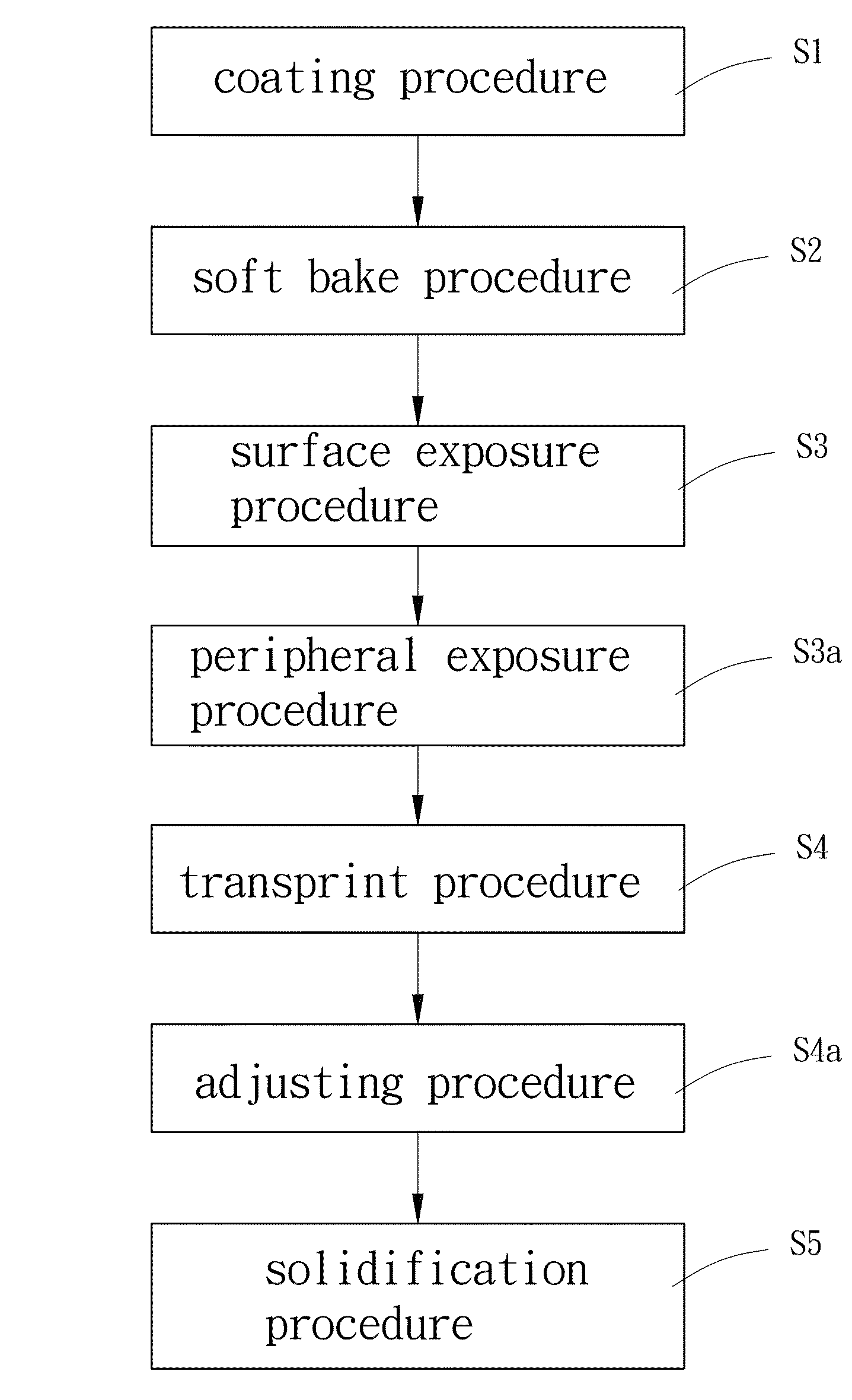
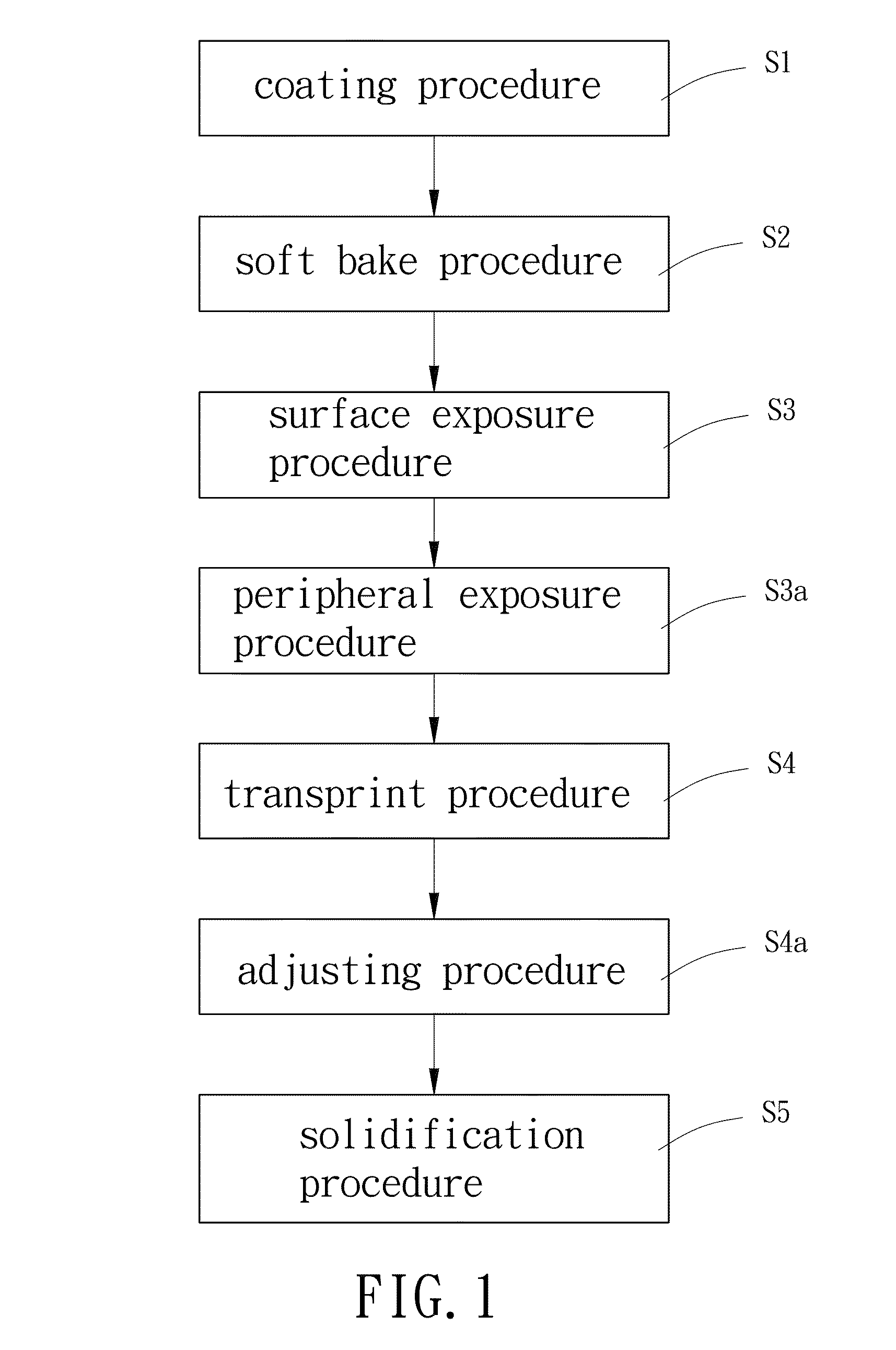
[0034]To make it easier for the objective of the invention, its structure, innovative features, and performance to be understood, reference is made to the following preferred embodiment together with the attached drawings for the detailed description of the invention.

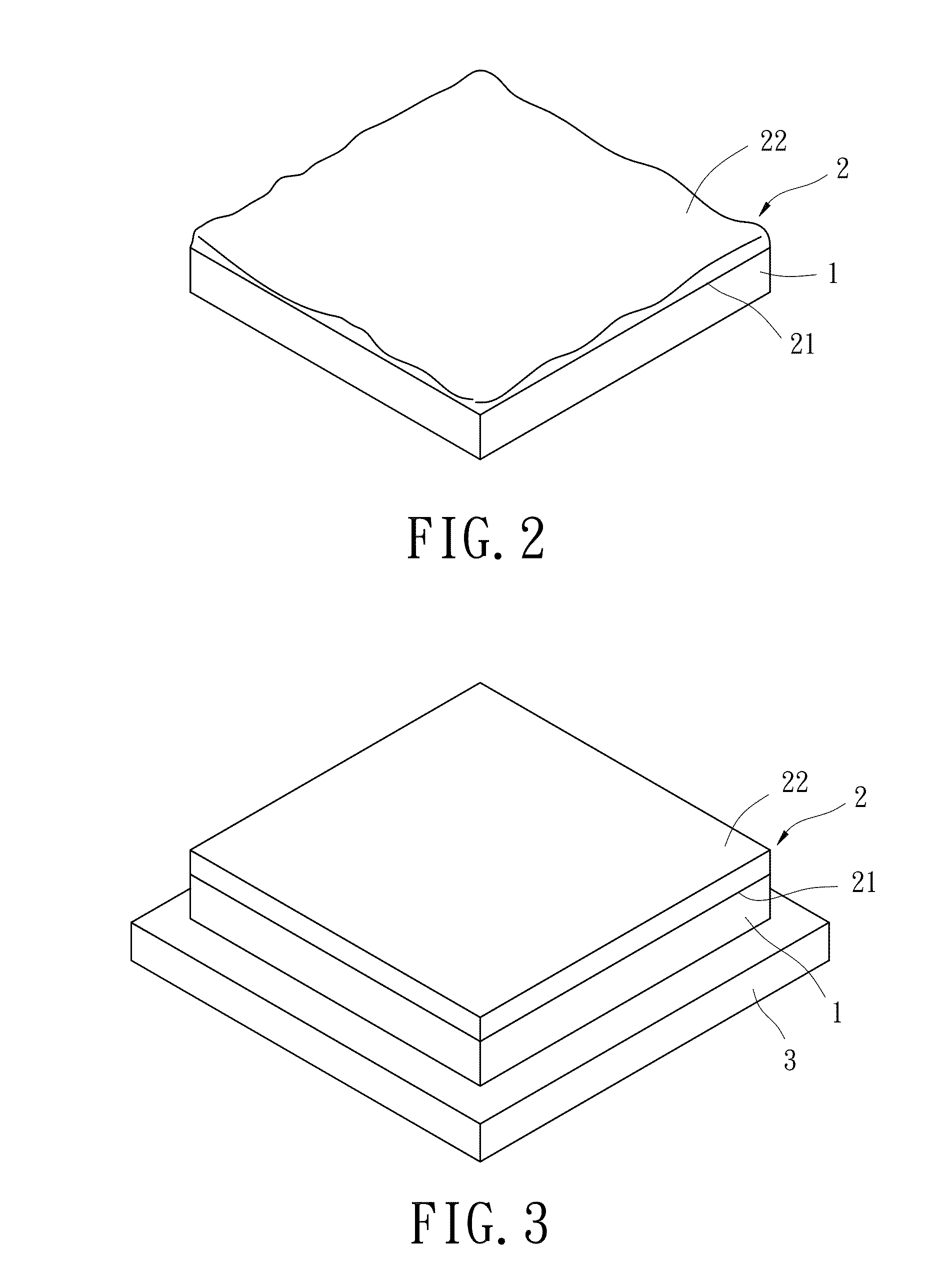
[0035]With reference to FIGS. 1 and 2, a coating procedure 51 is performed firstly. The photosensitive polymer is coated onto a surface of a first substrate 1 to form a polymer film 2, wherein the polymer film 2 has a first surface 21 and a second surface 22, and the first surface 21 is a surface of the polymer film 2 in contact with the first substrate 1. More specifically, the first substrate 1 can be made selectively of glass or another material, and it is preferable to wash the first substrate 1 before the polymer film is coated onto the first substrate 1 to keep impure substances from remaining on the surface of the first substrate 1. Secondly, a photosensitive polymer is coated onto the first substrate 1, wherein ...


PUM

PropertyMeasurementUnit
hole diameteraaaaaaaaaa
glass transition temperatureaaaaaaaaaa

Abstract

A method for manufacturing microlens comprises the steps of: coating a photosensitive polymer onto a first substrate to form a polymer film having a first surface in contact with the first substrate and a second surface; heating the polymer film; exposing the second surface of the polymer film to form a mold layer with at least one through hole; pressing and abutting the mold layer onto a second substrate and heating the photosensitive polymer within the mold layer to a temperature higher than a glass transition temperature of the photosensitive polymer for the photosensitive polymer to be melted and flow through the at least one through hole, attach onto the second substrate, and form at least one microlens on a surface of the second substrate; and performing an exposure to the at least one microlens and solidifying the at least one microlens.

Description

BACKGROUND OF THE INVENTION[0001]1. Field of the Invention[0002]This invention relates to a method of manufacturing a microlens, more particularly to a method of manufacturing a microlens array.[0003]2. Description of the Related Art[0004]Since microlens arrays are used extensively in optoelectronic industries for applications related to flat panel display, optical communication coupling, and near-field optical storage technologies, the microlens array manufacturing technology has become one of the major industrial developments.[0005]A conventional method of manufacturing a microlens array is disclosed in R.O.C. Publication No. 463058 entitled “Batch production of sphere microlens array,” and comprises the steps of: coating a first polymer onto a substrate; coating a second polymer onto the first polymer, wherein the first polymer has a glass transition temperature (Tg) greater than that of the second polymer; processing the first polymer and the second polymer by yellow light litho...

Claims


Application Information

Patent Timeline
Patent Type & Authority Patents(United States)
IPC IPC(8): B29D11/00
CPCB29D11/00365
Inventor LIN, CHE-HSINKUO, SHU-MING
Owner NAT SUN YAT SEN UNIV
Why Eureka
Try Eureka