Method of manufacturing semiconductor device and substrate processing apparatus

a technology of substrate processing and semiconductor devices, which is applied in the direction of liquid surface applicators, coatings, chemical vapor deposition coatings, etc., can solve the problems of difficult removal of organic metal liquid sources, and achieve the effect of suppressing the blockage of the inside of the flow passag

Active Publication Date: 2011-09-27
KOKUSA ELECTRIC CO LTD
View PDF7 Cites 15 Cited by
  • Summary
  • Abstract
  • Description
  • Claims
  • Application Information

AI Technical Summary

Benefits of technology

[0009]An object of the present invention is to provide a method of manufacturing a semiconductor device and a substrate processing apparatus capable of accelerating removal of the organic metal liquid source from the inside of the flow passage of the liquid source in the vaporizer, and suppressing blockade the inside of the flow passage of the liquid source.
[0025]According to the method of manufacturing the semiconductor device and the substrate processing apparatus of the present invention, it is possible to accelerate the removal of the organic metal liquid source from the inside of the flow passage of the liquid source in the vaporizer, and it is possible to suppress the blockage of the inside of the flow passage of the liquid source.

Problems solved by technology

Then, since the organic metal liquid source has high viscosity, it is difficult to remove the organic metal liquid source, even if the inert gas is supplied into the flow passage of the liquid source and the inside of the flow passage is purged.

Method used


Image

  • Method of manufacturing semiconductor device and substrate processing apparatus
  • Method of manufacturing semiconductor device and substrate processing apparatus
  • Method of manufacturing semiconductor device and substrate processing apparatus

Examples


first embodiment

(1) Structure of a Substrate Processing Apparatus

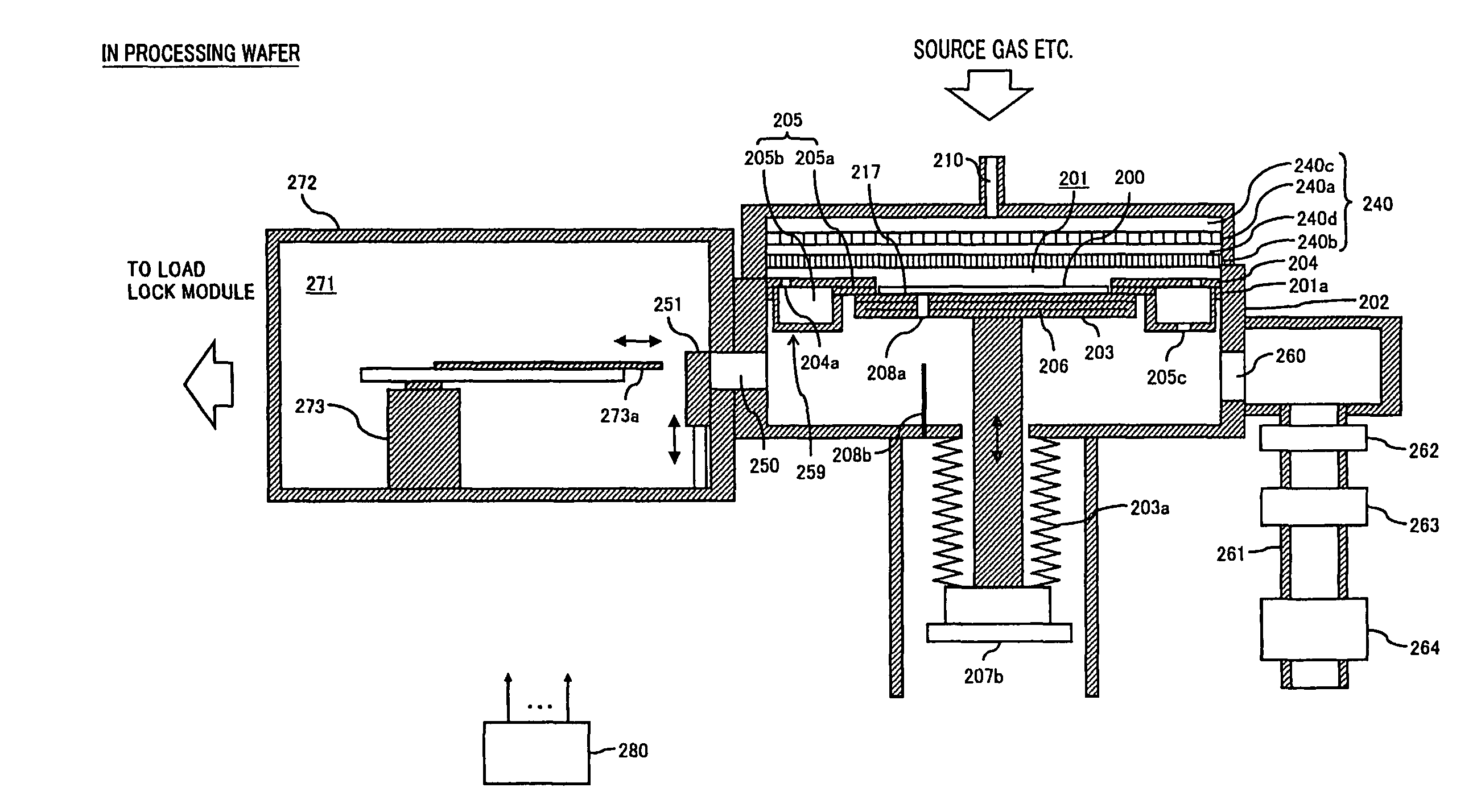
[0038]First, a structure of a substrate processing apparatus according to this embodiment will be explained, with reference to FIGS. 3 and 4. FIG. 4 is a sectional block diagram in transferring a wafer of the substrate processing apparatus according to a first embodiment of the present invention, and FIG. 3 is a sectional block diagram in processing the wafer of the substrate processing apparatus according to the first embodiment of the present invention.

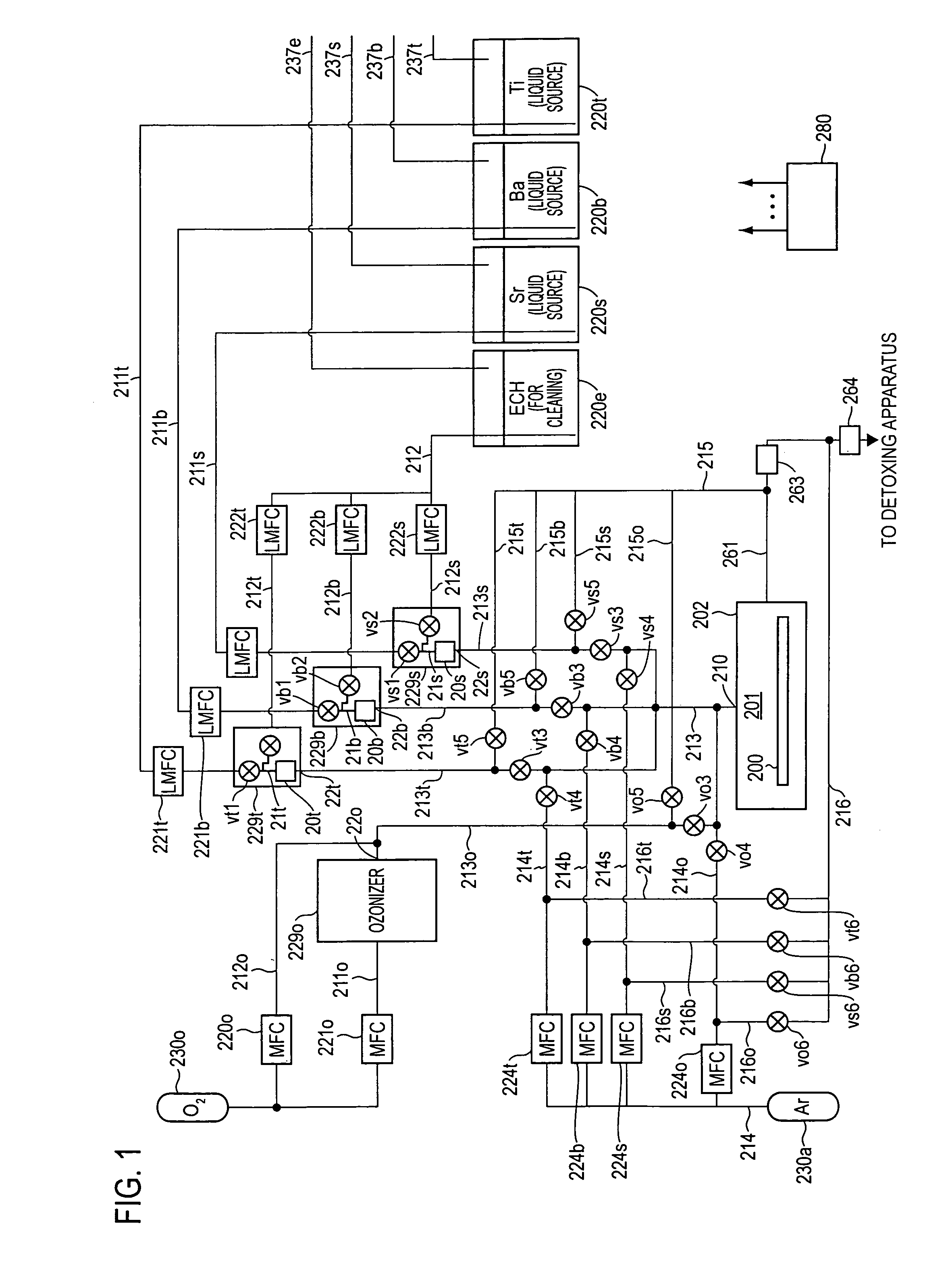
[0039]As shown in FIGS. 3 and 4, the substrate processing apparatus according to this embodiment includes a processing container 202. The processing container 202 is constituted as a flat air-tight container having a circular horizontal sectional face. Also, the processing container 202 is constituted of metal materials such as aluminum (Al) and stainless (SUS). A processing chamber 201 for processing a wafer 200 as a substrate is constituted in the processing container 202.

[0040]A su...

second embodiment

[0129]Next, the second embodiment of the present invention will be explained. According to the second embodiment, the aforementioned flushing operation, etc, will be mainly explained.

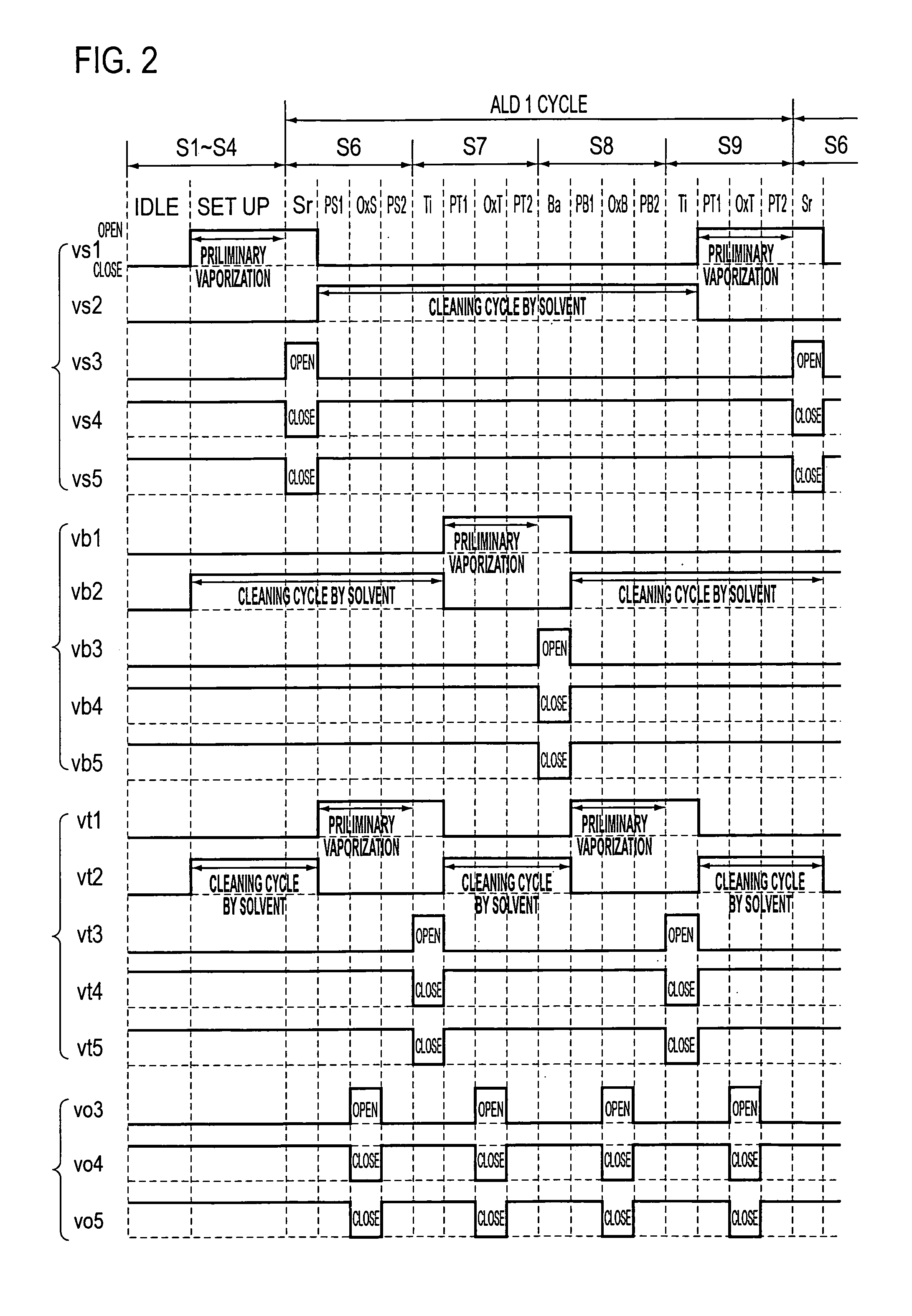
[0130]As described above, when the thin film containing the metal element is prepared in a semiconductor manufacturing step, the organic metal material obtained by chemically adding carbon, hydrogen, and nitrogen, etc, to metal atom, is used as a source in some cases. Vapor pressure is increased by using the organic metal, and the source can be treated as liquid at a temperature near normal temperature. Further, even in a case of the organic metal in a solid state at normal temperature and the liquid source having greatly high viscosity, it can be treated as the liquid of low viscosity by diluting (dissolving) in the solvent if solvable in the organic solvent and making a liquefied source (referred to as liquefied source hereunder). Such liquid source and liquefied source (in this specification, they ar...

third embodiment

[0168]Next, a third embodiment of the present invention will be explained. The aforementioned first embodiment and the second embodiment describe an example of depositing a film by using a sheet feeding type ALD apparatus for processing one sheet of substrate at a time, as the substrate processing apparatus. However, the present invention is not limited thereto. For example, a batch type vertical ALD apparatus for processing a plurality of substrates at a time may be used to deposit the film. This vertical ALD apparatus will be explained hereunder.

[0169]FIG. 7 is a schematic block diagram of a vertical type processing furnace of the vertical ALD apparatus suitable used in the third embodiment, FIG. 7A shows a vertical sectional face of a processing furnace 302 part, and FIG. 7B shows the sectional face of the processing furnace 302 part taken along the line A-A.

[0170]As shown in FIG. 7A, the processing furnace 302 has a heater 307 as a heating unit (heating mechanism). The heater 30...


PUM

PropertyMeasurementUnit
timeaaaaaaaaaa
timeaaaaaaaaaa
pressureaaaaaaaaaa

Abstract

A method of manufacturing a semiconductor device includes the steps of loading a substrate into a processing chamber; processing the substrate by supplying plural kinds of reaction substances into the processing chamber multiple number of times; and unloading the processed substrate from the processing chamber, wherein at least one of the plural kinds of reaction substances contains a source gas obtained by vaporizing a liquid source by a vaporizing part; in the step of processing the substrate, vaporizing operation of supplying the liquid source to the vaporizing part and vaporizing the liquid source is intermittently performed, and at least at a time other than performing the vaporizing operation of the liquid source, a solvent capable of dissolving the liquid source is flown to the vaporizing part at a first flow rate; and at a time other than performing the vaporizing operation of the liquid source and every time performing the vaporizing operation of the liquid source prescribed number of times, the solvent is flown to the vaporizing part at a second flow rate larger than the first flow rate.

Description

BACKGROUND[0001]1. Technical Field[0002]The present invention relates to a method of manufacturing a semiconductor device for processing a substrate by a source gas obtained by vaporizing liquid source, and a substrate processing apparatus.[0003]2. Description of Related Art[0004]As a method of forming a thin film by atomic layer unit on a substrate such as a wafer, a so-called ALD (Atomic Layer Deposition) is used. In the ALD method, for example, (1) the step of supplying a first processing gas into a processing chamber in which the substrate is contained and making the first processing gas adsorbed on the surface of the substrate, (2) the step of introducing inert gas into the processing chamber to remove the first processing gas remained in the processing chamber and purging an inside of the processing chamber, (3) the step of supplying a second processing gas into the processing chamber and causing reaction to occur between the second processing gas and the first processing gas ...

Claims


Application Information

Patent Timeline
Patent Type & Authority Patents(United States)
IPC IPC(8): H01L21/00C23C16/00
CPCC23C16/409C23C16/4401C23C16/4412C23C16/45531C23C16/45534C23C16/45561C23C16/45565H01L21/3141H01L21/31691H01L21/02197H01L21/0228H01L21/02H01L21/20C23C16/45525
Inventor HORII, SADAYOSHIIMAI, YOSHINORI
Owner KOKUSA ELECTRIC CO LTD
Why Eureka
Try Eureka