Liquid crystal display panel having a touch function
a technology of liquid crystal display panel and touch function, which is applied in non-linear optics, instruments, optics, etc., can solve the problems of increasing manufacture time and cost, and achieve the effect of reducing the weight of the liquid crystal display panel and not increasing the manufacture time and cos
- Summary
- Abstract
- Description
- Claims
- Application Information
AI Technical Summary
Benefits of technology
Problems solved by technology
Method used
Image

Examples
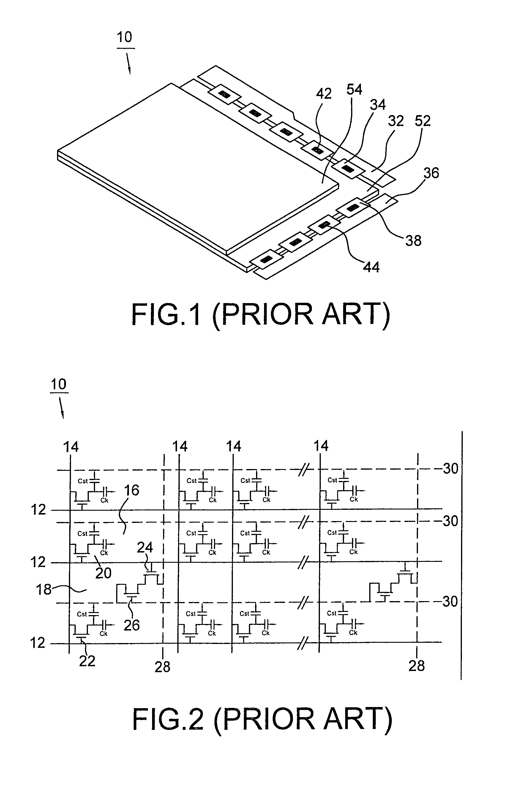
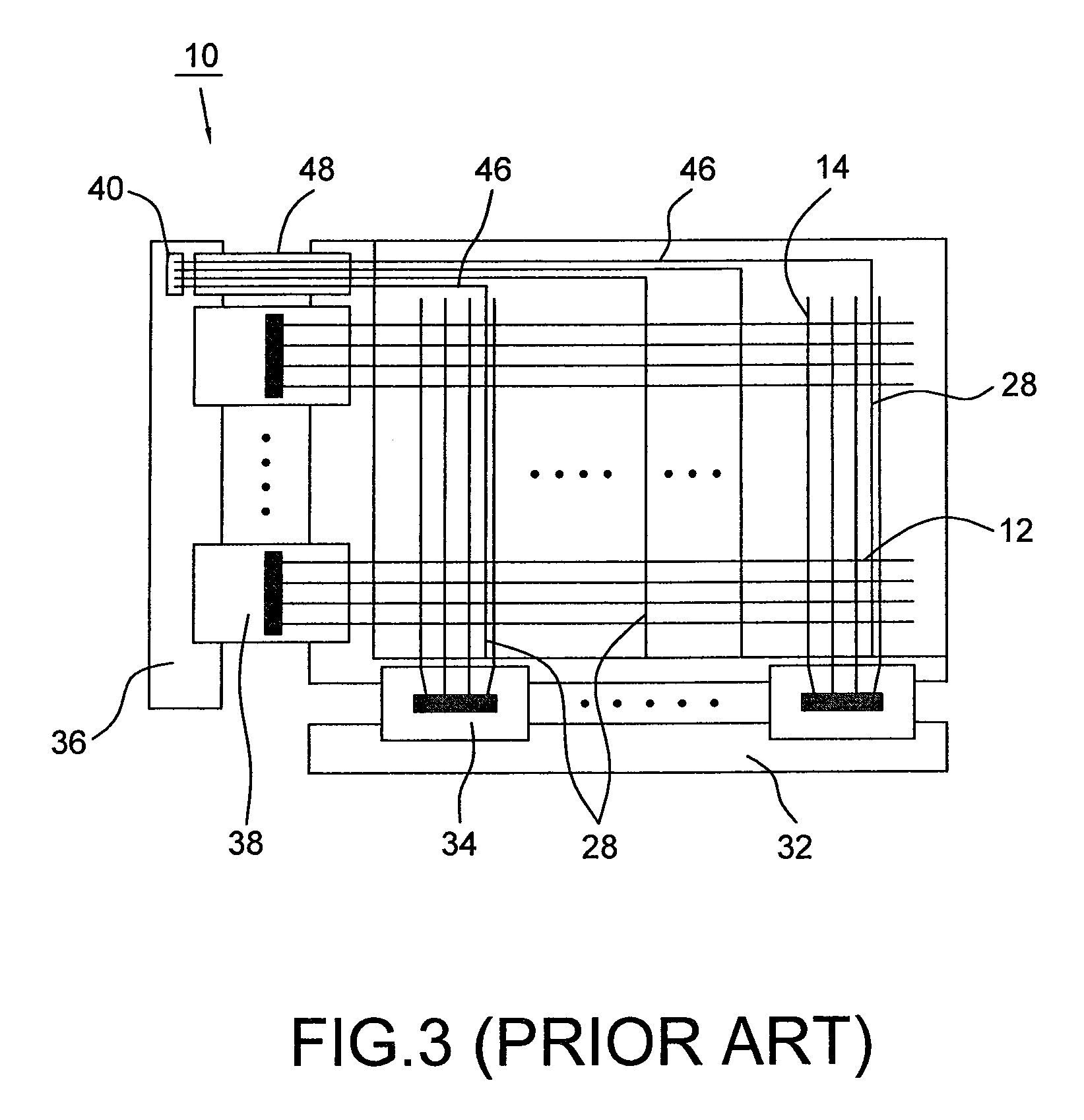
first embodiment
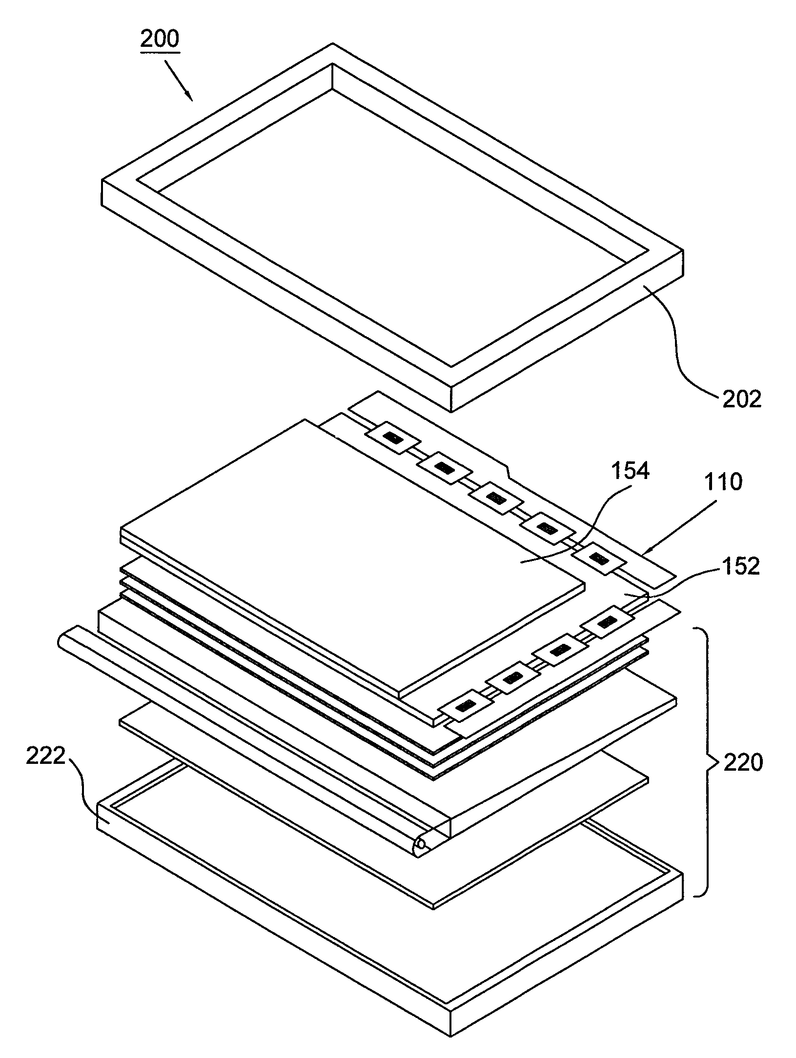
[0029]Referring to FIG. 5, it depicts a liquid crystal display panel 110 having a touch function according to the present invention, e.g. a liquid crystal display panel having an optical touch component. The liquid crystal display panel 110 includes a data printed circuit board (data PCB) 132, a plurality of first connection units 134 (e.g. a data chip on film package, i.e. Data COF Package), and a plurality of second connection units 138 (e.g. a gate chip on film package, i.e. Gate COF Package, or a gate chip on glass package, i.e. Gate COG Package). Each first connection unit 134 is electrically connected to the data PCB 132 and a periphery region of a long side of the lower substrate 152 and includes a data driver 142. Each second connection unit 138 is electrically connected to a periphery region of a short side of the lower substrate 152 and includes a gate driver 144. The first and second connection units 134, 138 further includes flexible boards 135, 139 respectively, wherein...
second embodiment
[0036]Referring to FIG. 8, it depicts a liquid crystal display panel 310 according to the present invention. The liquid crystal display panel 310 includes a data PCB 332, a plurality of first connection units 334 (e.g. a data driver 342 and a flexible board 335 are combined to the first connection unit 334), and a plurality of second connection units 338 (e.g. a gate chip on film package, i.e. Gate COF Package, or a gate chip on glass package, i.e. Gate COG Package). Each first connection unit 334 is electrically connected to the data PCB 332 and a periphery region of a long side of the lower substrate 352 and includes the data driver 342 and flexible board 335. It is noted that the data driver 342 is mounted on the lower substrate 352 rather than the flexible board 335. Each second connection unit 338 is electrically connected to a periphery region of a short side of the lower substrate 352 and includes a gate driver 344 and flexible board 339, wherein the gate driver 344 is mounte...
PUM
| Property | Measurement | Unit |
|---|---|---|
| flexible | aaaaa | aaaaa |
| conductive | aaaaa | aaaaa |
| resistance | aaaaa | aaaaa |
Abstract
Description
Claims
Application Information
 - R&D
- Intellectual Property
- Life Sciences
- Materials
- Tech Scout
- Unparalleled Data Quality
- Higher Quality Content
- 60% Fewer Hallucinations
Browse by: Latest US Patents, China's latest patents, Technical Efficacy Thesaurus, Application Domain, Technology Topic, Popular Technical Reports.
© 2025 PatSnap. All rights reserved.Legal|Privacy policy|Modern Slavery Act Transparency Statement|Sitemap|About US| Contact US: help@patsnap.com