Rinse method and developing apparatus

a technology of developing apparatus and rinsing method, which is applied in the direction of cleaning process and apparatus, chemistry apparatus and processes, cleaning using liquids, etc., can solve the problems of reducing product yield, reducing the accuracy of development defects, and the inability to accurately measure development defects with surface inspection apparatus or the like, so as to reduce the number of development defects.

Inactive Publication Date: 2011-10-04
TOKYO ELECTRON LTD
View PDF7 Cites 0 Cited by
  • Summary
  • Abstract
  • Description
  • Claims
  • Application Information

AI Technical Summary

Benefits of technology

[0009]It is an object of the invention to provide a rinse method capable of promptly grasping a condition which reduces development defects regardless of a target substrate and performing a rinse process after a developing process.
[0018]To overcome the problems, the present inventors grasped the behavior of the occurrence of development defects for substrates with various surface states, and discovered that the behavior of the occurrence of development defects significantly depend on the surface state of a substrate after development. According to the invention, therefore, rinse conditions are preset according to surface states of a substrate, the surface state of a substrate is measured, a rinse condition corresponding to the measured surface state of the substrate is selected, and a rinse process is performed under the selected condition. Provided that the optimal rinse conditions which hardly cause development defects are set in association with individual substrate surface states, if just the surface state of a substrate is grasped, the optimal rinse condition corresponding to the surface state can be selected quickly, and a rinse process for the substrate can be performed under the condition. This makes it possible to promptly grasp the optimal condition regardless of a target substrate and perform a rinse process with fewer development defects.

Problems solved by technology

If the process is done insufficiently, multiple development defects occur, thus reducing the product yield.
Japanese Patent Laid-Open Publication No. 2002-57093 describes that a method of actually measuring development defects with a surface inspection apparatus or the like may not be able to provide highly reliable measurements, and the apparatus is expensive, and discloses, as a technique of avoiding such an inconvenience, a method of immersing the surface of a substrate in a pre-process liquid to dissolve the components in the developer adhered to the surface of the substrate into the pre-process liquid after a post-development rinse process is performed, analyzing the pre-process liquid to quantitatively analyze the components in the developer to thereby grasp development defects, and setting the time or the like of supplying the rinse liquid based on the analysis result.
Even if this method of grasping development defects is employed, however, the condition that reduces development defects differs depending on the material of a resist to which the developer is applied, and the condition needs to be set again every time the material is changed, thereby increasing the number of working steps required to set up the apparatus.
The work of setting the condition after grasping development defects should not necessarily find an optimal condition.

Method used


Image

  • Rinse method and developing apparatus
  • Rinse method and developing apparatus
  • Rinse method and developing apparatus

Examples


Embodiment Construction

[0037]An embodiment of the present invention will be described in detail below with reference to the accompanying drawings.

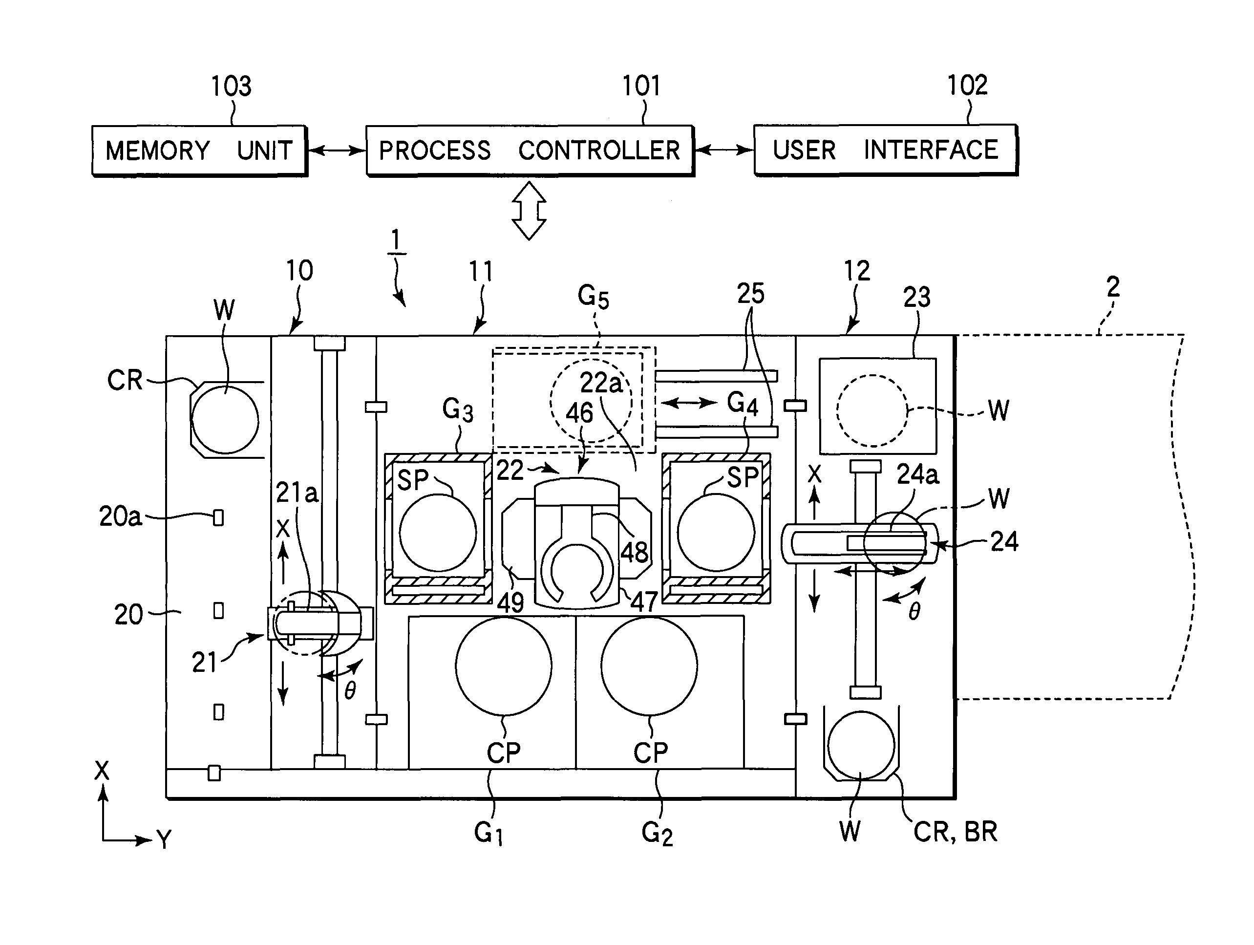
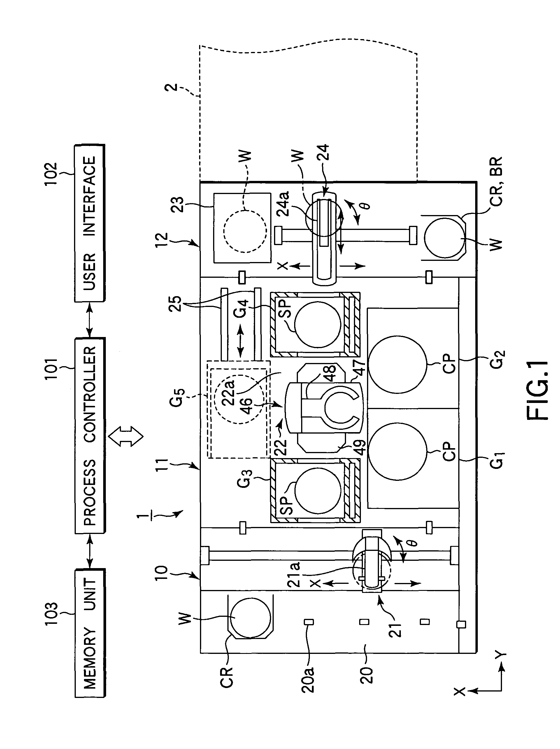
[0038]FIG. 1 is a schematic plan view showing a resist coating and developing system provided with a developing apparatus which executes the rinse method of the present invention, FIG. 2 is a front view thereof, and FIG. 3 is a rear view thereof.

[0039]This resist coating and developing system 1 comprises a cassette station 10 as a transfer station, a process station 11 having a plurality of process units, and an interface section 12 for transferring a wafer W to an exposure apparatus 2 provided adjacent to the process station 11.

[0040]The cassette station 10 transfers a wafer cassette CR where a plurality of wafers W as subjects to be processed are placed into and out of this system. In the cassette station 10, as shown in FIG. 1, four positioning projections 20a are formed along an X direction in the diagram on a placing table 20 on which wafer cassettes CR are...


PUM


Abstract

A rinse method for rinsing a substrate having an exposure pattern thereon developed includes presetting conditions for a rinse process according to surface states of the substrate, measuring a surface state of the substrate, selecting a corresponding condition for the rinse process based on the measured surface state of the substrate, and performing the rinse process under the selected condition.

Description

BACKGROUND OF THE INVENTION[0001]1. Field of the Invention[0002]The present invention relates to a rinse method which performs a rinse process on a substrate, such as a semiconductor wafer, after an exposure pattern is developed, a developing apparatus which performs such a rinse process, and a computer readable storage medium.[0003]2. Description of the Related Art[0004]In semiconductor device fabrication process, for example, a resist pattern is formed as a mask for forming a predetermined pattern by a so-called photolithography technology in which after a resist liquid is supplied to the top surface of a semiconductor wafer (hereinafter called “wafer”) to form a resist film, and an exposure process is performed on a resist-coated wafer according to a predetermined pattern, an exposure pattern formed on the resist film on the wafer is developed.[0005]In the developing process included in the individual processes of such a photolithography technique, a developing unit (DEV) is supp...

Claims


Application Information

Patent Timeline
Patent Type & Authority Patents(United States)
IPC IPC(8): B08B7/04
CPCH01L21/67253H01L21/67051B08B3/02G03F7/40H01L21/02057
Inventor YOSHIHARA, KOUSUKENAKAMURA, JUNJITAKEGUCHI, HIROFUMIYAMAMOTO, TARO
Owner TOKYO ELECTRON LTD
Why Eureka
Try Eureka