Method for manufacturing display device

a display device and manufacturing method technology, applied in semiconductor devices, optics, instruments, etc., can solve the problems of difficult to further reduce the number of photomasks, and achieve the effects of reducing yield and reliability, reducing leakage current generated between a gate electrode and a drain electrode, and simplifying the manufacturing process of a display devi

Inactive Publication Date: 2011-10-11
SEMICON ENERGY LAB CO LTD
View PDF23 Cites 4 Cited by
  • Summary
  • Abstract
  • Description
  • Claims
  • Application Information

AI Technical Summary

Benefits of technology

[0037]In addition to the above advantageous effects, a thin film transistor included in a display device is mechanically stable; therefore, a manufacturing process of a display device can be simplified without reducing yield and reliability.
[0038]Note that a thin film transistor manufactured by the invention to be disclosed has a cavity adjacent to an end portion of a gate electrode layer; therefore, a leakage current generated between a gate electrode and a drain electrode is small.

Problems solved by technology

However, even in the case where a bottom gate thin film transistor is manufactured using the above multi-tone mask, one photomask is required to be used for patterning a gate electrode layer and it has been difficult to further reduce the number of photomasks.

Method used


Image

  • Method for manufacturing display device
  • Method for manufacturing display device
  • Method for manufacturing display device

Examples


embodiment mode 1

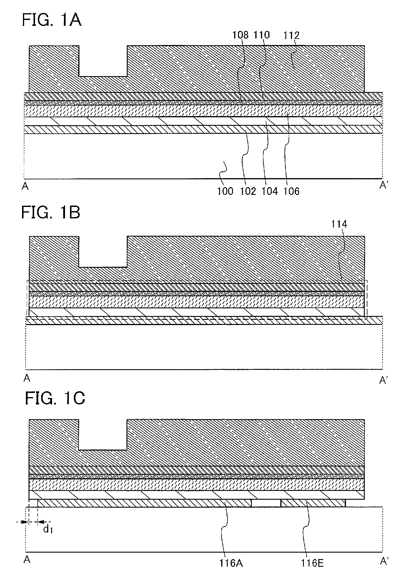
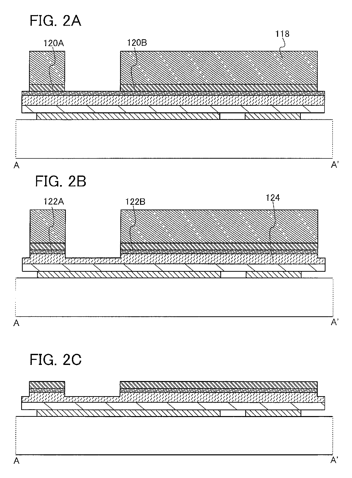
[0085]In this embodiment mode, an example of a method for manufacturing a thin film transistor and an example of a method for manufacturing a display device in which thin film transistors obtained by the above method are arranged in matrix will be described with reference to FIGS. 1A to 1C, FIGS. 2A to 2C, FIGS. 3A to 3C, FIGS. 4A to 4C, FIGS. 5A to 5C, FIGS. 6A to 6C, FIGS. 7A to 7C, FIGS. 8A to 8C, FIGS. 9A to 9C, FIGS. 10A to 10C, FIGS. 11A to 11C, FIGS. 12A to 12C, FIGS. 13A to 13C, FIGS. 14A to 14C, FIGS. 15A to 15C, FIG. 16, FIG. 17. FIG. 18, FIG. 19, FIG. 20, FIG. 21, FIG. 22, FIGS. 23A to 23C, FIGS. 24A-1 to 24B-2, FIG. 25, FIG. 26, and FIG. 27.

[0086]Note that FIG. 16, FIG. 17, FIG. 18, FIG. 19, and FIG. 20 illustrate top plan views of a thin film transistor according to this embodiment mode, and FIG. 20 is a completion view in which components are formed up to a pixel electrode. FIGS. 1A to 1C, FIGS. 2A to 2C, and FIGS. 3A to 3C are cross-sectional views along A-A′ in FIG. ...

embodiment mode 2

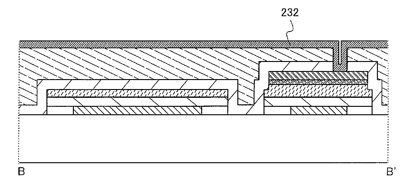
[0193]In this embodiment mode, a different mode from Embodiment Mode 1 is described with reference to FIGS. 28A to 28C, FIGS. 29A to 29C, FIGS. 30A to 30C, FIGS. 31A to 31C, FIGS. 32A to 32C, FIGS. 33A to 33C, FIG. 34, FIG. 35, FIG. 36, FIG. 37, FIG. 38, FIG. 39, FIG. 40, and FIG. 41.

[0194]Note that FIG. 34, FIG. 35, FIG. 36, FIG. 37, and FIG. 38 illustrate top plan views of a thin film transistor according to this embodiment mode, and FIG. 38 is a completion view in which components are formed up to a pixel electrode. FIGS. 28A to 28C, FIGS. 29A to 29C, and FIGS. 30A to 30C are cross-sectional views along A-A′ in FIG. 34, FIG. 35, FIG. 36, FIG. 37, and FIG. 38. FIGS. 31A to 31C, FIGS. 32A to 32C, and FIGS. 33A to 33C are cross-sectional views along B-B′ in FIG. 34, FIG. 35, FIG. 36, FIG. 37, and FIG. 38.

[0195]First, a first conductive film 202, a first insulating film 204, a semiconductor film 206, an impurity semiconductor film 208, and a second conductive film 210 are formed over...

embodiment mode 3

[0250]In this embodiment mode, electronic appliances in each of which a display panel or a display device manufactured by any of the methods described in Embodiment Modes 1 and 2 is incorporated as a display portion will be described with reference to FIGS. 42A and 42B, FIG. 43, and FIGS. 44A to 44C. As such electronic appliances, for example, cameras such as video cameras or digital cameras; head mounted displays (goggle type displays); car navigation systems; projectors; car stereos; personal computers; and portable information terminals (such as mobile computers, mobile phones, and e-book readers) can be given. Examples of the electronic appliances are illustrated in FIGS. 42A and 42B.

[0251]FIG. 42A illustrates a television device. A television device illustrated in FIG. 42A can be completed by incorporating a display panel manufactured using the invention to be disclosed into a housing. A main screen 323 is formed using the display panel manufactured by any of the manufacturing ...


PUM

PropertyMeasurementUnit
thicknessaaaaaaaaaa
transmittanceaaaaaaaaaa

Abstract

A first conductive film, a first insulating film, a semiconductor film, an impurity semiconductor film, a second conductive film, and a first resist mask are formed; first etching is performed to expose at least a surface of the first conductive film; second etching accompanied by side etching is performed on part of the first conductive film to form a gate electrode layer; a second resist mask is formed; third etching is performed to form a source and drain electrode layers, a source and drain regions, and a semiconductor layer; a second insulating film is formed; an opening portion is formed in the second insulating film to partially expose the source or drain electrode layer; a pixel electrode is selectively formed in the opening portion and over the second insulating film; and a supporting portion formed using the gate electrode layer is formed in a region overlapping with the opening portion.

Description

BACKGROUND OF THE INVENTION[0001]1. Field of the Invention[0002]The present invention relates to a method for manufacturing a display device.[0003]2. Description of the Related Art[0004]In recent years, thin film transistors each formed using a semiconductor thin film with a thickness of several nm to several hundred nm over a substrate having an insulating surface, such as a glass substrate, have attracted attention. Thin film transistors have been widely used for ICs (integrated circuits) and electronic devices typified by electrooptic devices. Thin film transistors have been rapidly developed particularly as switching elements for display devices typified by liquid crystal display devices, EL (electroluminescent) display devices, and the like. In an active matrix liquid crystal display device, a voltage is applied between a selected pixel electrode connected to a switching element and a counter electrode corresponding to the selected pixel electrode, whereby a liquid crystal laye...

Claims


Application Information

Patent Timeline
Patent Type & Authority Patents(United States)
IPC IPC(8): H01L29/786G02F1/1368H01L21/336
CPCH01L27/1288H01L21/764
Inventor MIZOGUCHI, TAKAFUMIMIKAMI, MAYUMISAITO, YUMIKO
Owner SEMICON ENERGY LAB CO LTD
Why Eureka
Try Eureka