Supercharge Your Innovation With Domain-Expert AI Agents!

Semiconductor device with deep trench structure

a technology of semiconductor devices and trenches, which is applied in the direction of semiconductor devices, electrical equipment, transistors, etc., can solve the problems of increasing power consumption of control circuits and the size of tft-lcd, and difficulty in separating neighboring wells from each other, so as to reduce the size of the semiconductor device and reduce the cos

Active Publication Date: 2011-11-01
KEY FOUNDRY CO LTD
View PDF16 Cites 3 Cited by
  • Summary
  • Abstract
  • Description
  • Claims
  • Application Information

AI Technical Summary

Benefits of technology

"The present invention provides a semiconductor device with a deep trench structure and a method of manufacturing the same for effectively isolating wells of PMOS and NMOS regions from each other. The semiconductor device includes a first isolation layer having a deep trench structure and isolating the first and second conductivity type wells from each other. The method includes forming a first isolation layer, a second isolation layer with a shallower trench structure, drift regions in the wells, and source and drain regions. The technical effect of the invention is to isolate heavily doped wells and reduce the size and cost of the semiconductor device."

Problems solved by technology

The control circuit has a logic circuit operating at 5V and the driving circuit has a high voltage transistor operating at higher than 30V, and thus the TFT-LCD cannot be manufactured using a standard complementary metal oxide semiconductor (CMOS) process.
Furthermore, when a high voltage device manufacturing process is applied to the TFT-LCD, power consumption of the control circuit and the size of the TFT-LCD increase.
In this case, it is difficult to isolate neighboring wells from each other as an operating voltage of the high voltage element increases.
This increase the size of the high voltage device, and thus the high voltage device is not suitable for a driving IC.
That is, the increase in the size of the high voltage device causes an increase in the device cost and deterioration of integration, and thus the high voltage device is not suitable to be used as a driving IC because current devices require a small size, high integration and low cost.

Method used


Image

  • Semiconductor device with deep trench structure
  • Semiconductor device with deep trench structure
  • Semiconductor device with deep trench structure

Examples


Embodiment Construction

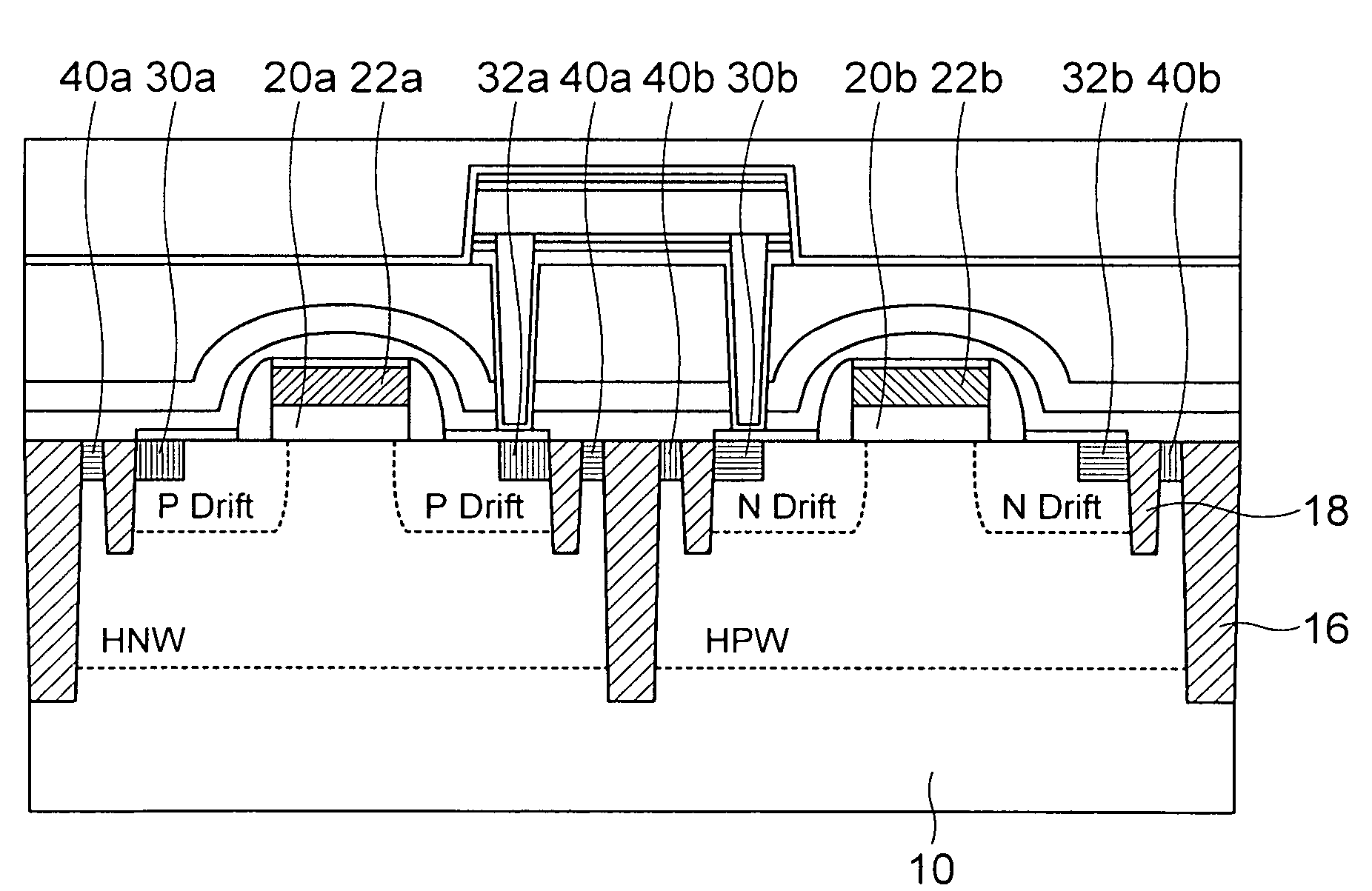
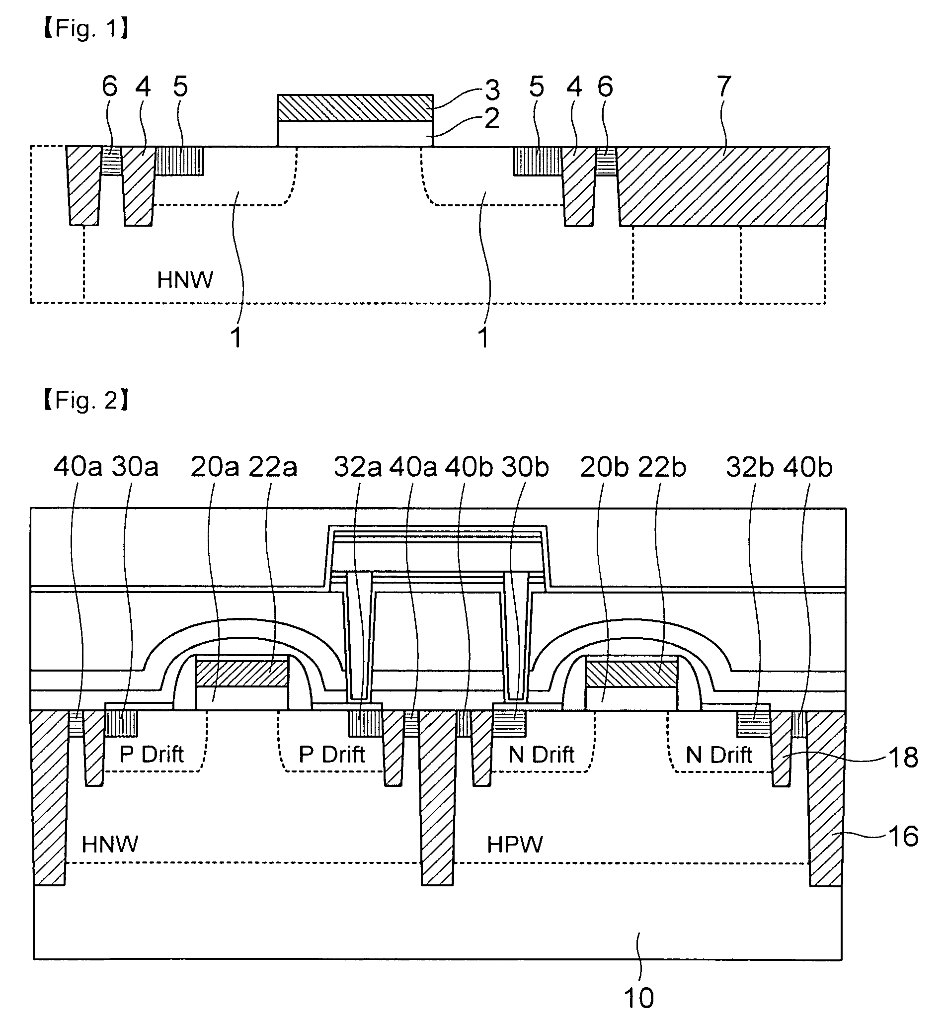
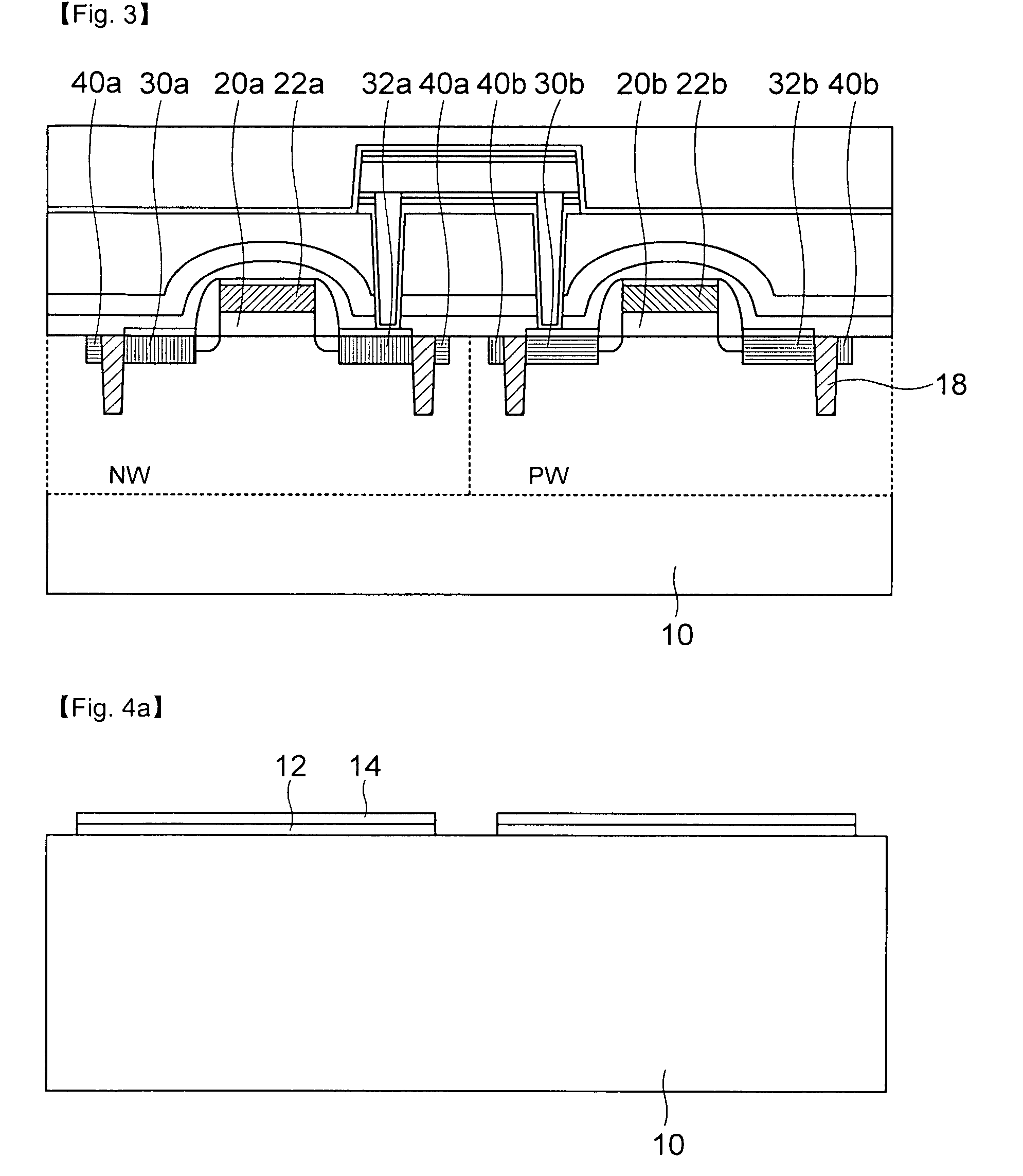
[0026]FIG. 2 is a cross-sectional view illustrating a high voltage region of a semiconductor device with a deep trench structure according to an embodiment of the present invention and FIG. 3 is a cross-sectional view illustrating a low voltage region of the semiconductor device with a deep trench structure illustrated in FIG. 2. Detailed explanation of the low voltage region will be omitted.

[0027]Referring to FIG. 2, a semiconductor substrate 10 is divided into a PMOS region and an NMOS region according to a first isolation layer 16 having a deep trench structure and an N well HNW and a P well HPW of opposite conductivity types are respectively formed in the PMOS region and the NMOS region. A gate oxide film 20a and a gate electrode 22a are laminated on the N well HNW and a gate oxide film 20b and a gate electrode 22b are laminated on the P well HPW.

[0028]P type drift regions P Drift doped with ions having conductivity opposite to the N well HNW are respectively formed on both side...


PUM


Abstract

Disclosed herein is a semiconductor device with a deep trench structure for effectively isolating heavily doped wells of neighboring elements from each other at a high operating voltage. The semiconductor device with a deep trench structure includes a semiconductor substrate in which a first conductivity type well and a second conductivity type well having conductivity opposite to that of the first conductivity type well are formed, a gate oxide film and a gate electrode laminated on each of the first conductivity type well and the second conductivity type well, second conductivity type drift regions formed on both sides of the gate electrode formed on the first conductivity type well, first conductivity type drift regions formed on both sides of the gate electrode formed on the second conductivity type well, and a first isolation layer having a trench structure deeper than the first and second conductivity type wells and isolating the first conductivity type well and the second conductivity type well from each other.

Description

CROSS-REFERENCE TO RELATED APPLICATION[0001]This application claims the benefit under 35 U.S.C. §119(a) of Korean Patent Application No. 10-2007-140352 filed on Dec. 28, 2007, in the Korean Intellectual Property Office, the entire disclosure of which is incorporated herein by reference for all purposes.BACKGROUND OF THE INVENTION[0002]1. Field of the Invention[0003]The present invention relates to a semiconductor device with a deep trench structure and, more particularly, to a semiconductor device with a deep trench structure for effectively isolating heavily doped wells of neighboring elements from each other at a high operating voltage.[0004]2. Background of the Related Art[0005]As integrated circuits having various functions coexist in the same product because of high integration of semiconductor circuits, a multi-voltage / current driving high voltage transistor is required.[0006]A thin film transistor-liquid crystal display (TFT-LCD) includes a driving circuit and a control circu...

Claims


Application Information

Patent Timeline
Patent Type & Authority Patents(United States)
IPC IPC(8): H01L27/092
CPCH01L29/0653H01L29/6659H01L29/7833H01L29/1087H01L21/76
Inventor KIM, DO HYUNGLIM, YONG GYU
Owner KEY FOUNDRY CO LTD
Features
  • R&D
  • Intellectual Property
  • Life Sciences
  • Materials
  • Tech Scout
  • Unparalleled Data Quality
  • Higher Quality Content
  • 60% Fewer Hallucinations
Learn More