Directed reagents to improve material uniformity

a technology of reagents and uniformity, applied in the direction of polycrystalline material growth, crystal growth process, condensed vapor, etc., can solve the problem of low nitrogen dopant incorporation efficiency

Active Publication Date: 2011-11-08
CREE INC
View PDF38 Cites 225 Cited by
  • Summary
  • Abstract
  • Description
  • Claims
  • Application Information

AI Technical Summary

Problems solved by technology

A higher silicon to carbon ratio in the process gas may result in higher nitrogen (donor) dopant incorporation efficiency during silicon carbide growth, while a lower silicon to carbon ratio in the process gas may result in lower nitrogen dopant incorporation efficiency.

Method used


Image

  • Directed reagents to improve material uniformity
  • Directed reagents to improve material uniformity
  • Directed reagents to improve material uniformity

Examples


example 1

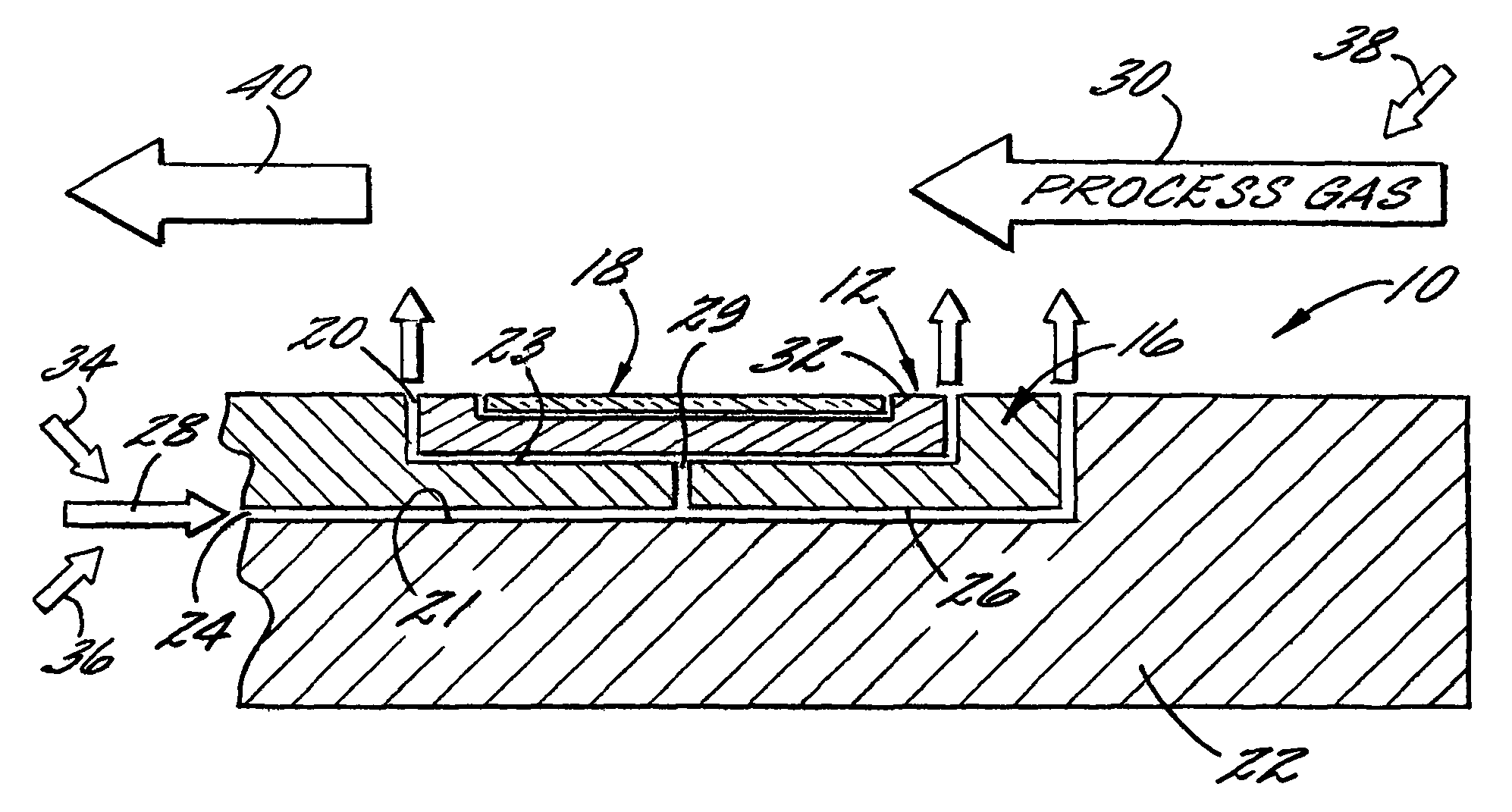
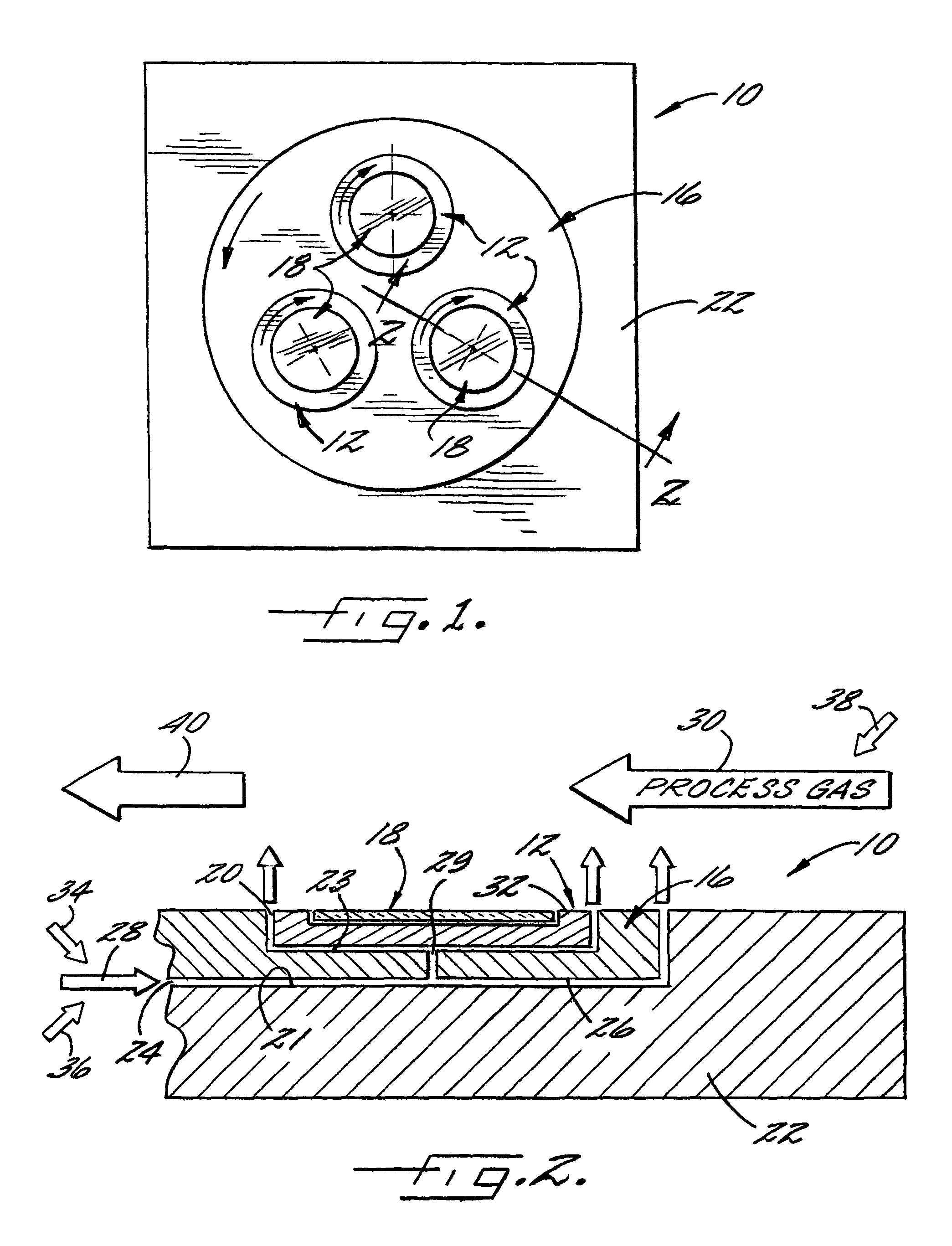
[0043]A measure of graphite dust was placed in the “moat” area (e.g., the indented top surface of a platter) to allow local introduction of a carbon rich gas through reaction with H2 in the carrier gas at the wafer edge. After loading three wafers into the system, one wafer in the satellite surrounded by the dust and two wafers in satellites removed from the dust, SiC MESFET epitaxial structures were grown on all three wafers. The doping in the center of each wafer was approximately the same. The doping profiles, however, revealed a 6% average doping increase on the edge of the wafer processed while surrounded by the dust filled moat, while the wafers processed near standard moats demonstrated 12% and 16% dopant incorporation increase on the wafer edges, respectively. This example demonstrates the ability to locally control the stoichiometry, as well as the dopant incorporation levels, by introducing a second reactant near the wafer edge.

example 2

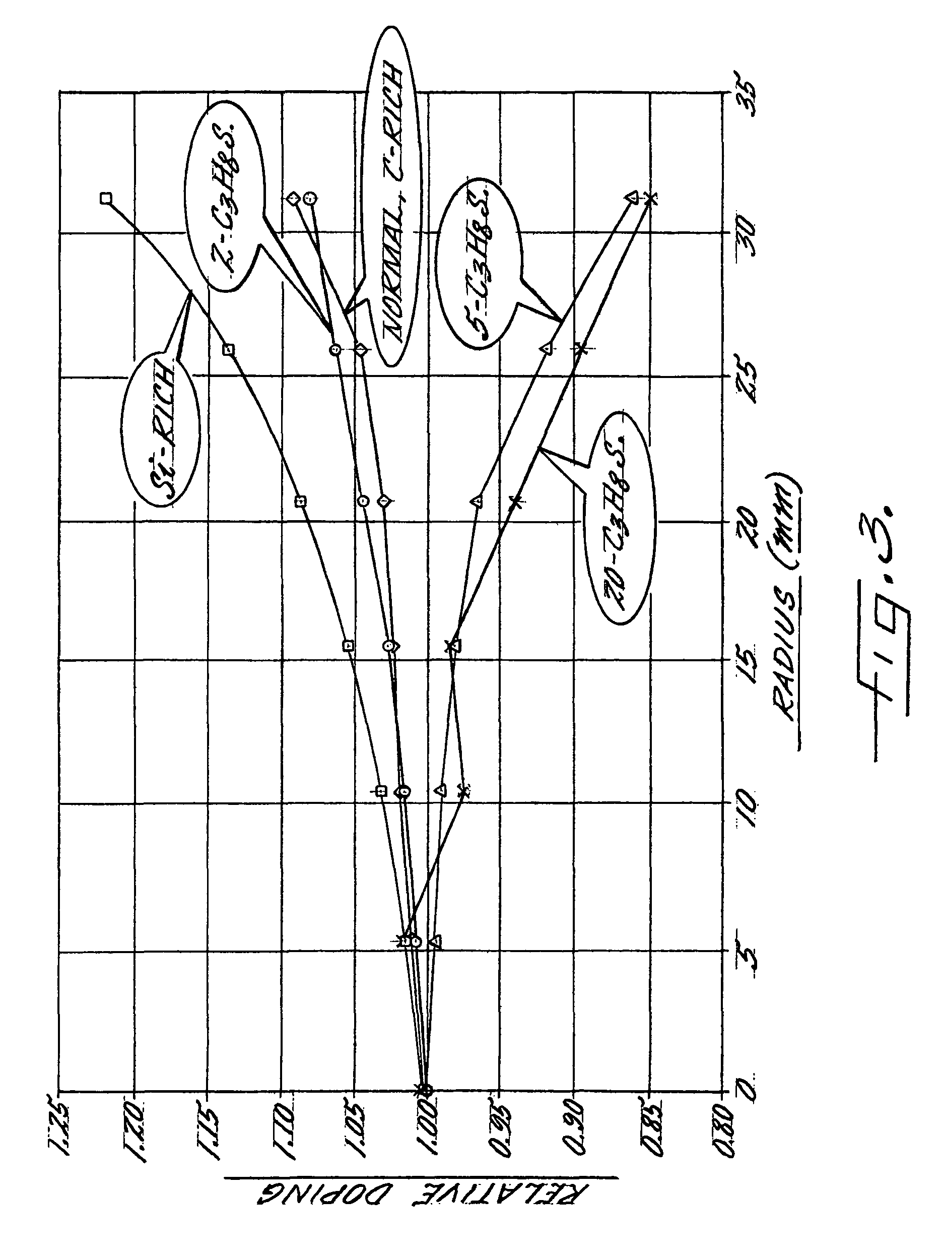
[0044]With reference to FIG. 3, a series of tests were conducted, with a reaction environment ranging from silicon-rich to carbon-rich. FIG. 3 is a graph representing the cross-wafer doping profile of the various tests. The x-axis of the table represents the wafer radius in millimeters, with 0 being the center of the wafer and 35 being the perimeter of the wafer. The y-axis of the table represents relative nitrogen dopant incorporation. To take advantage of the improved stoichiometry control provided by the present invention, five different tests were run, beginning with a silicon-rich reactant stream, followed by including propane in the drive gas stream in amounts of 2, 5, and 20 sccm as seen in the respective curves. As is known in the art, sccm is the abbreviation for a standard cubic centimeter per minute. Stated differently, one sccm is one cubic centimeter of gas per minute at 0° C. and atmospheric pressure. As can be seen in FIG. 3, the cross wafer doping trend inverts betwe...


PUM

PropertyMeasurementUnit
n-type conductivityaaaaaaaaaa
temperatureaaaaaaaaaa
chemical concentrationaaaaaaaaaa

Abstract

A method for locally controlling the stoichiometry of an epitaxially deposited layer on a semiconductor substrate is provided. The method includes directing a first reactant gas and a doping gas across a top surface of a semiconductor substrate and directing a drive gas and a second reactant gas against the substrate separately from the first reactant gas in a manner that rotates the substrate while introducing the second reactant gas at an edge of the substrate to control each reactant separately, thereby compensating and controlling depletion effects and improving doping uniformity in resulting epitaxial layers on the substrate.

Description

BACKGROUND OF THE INVENTION[0001]The present invention relates to methods and apparatus for depositing epitaxial layers on wafers and other substrates, and more particularly, to improving the doping uniformity and related qualities of such layers.[0002]The semiconductor industry employs crystal growth from vapor, in particular, for producing epitaxial layers on semiconductor wafers. The term epitaxy typically describes the growth of a monocrystalline layer on the planar boundary surface of a monocrystalline substrate, generally a substrate wafer of a semiconductor material.[0003]Epitaxial growth is often carried out using chemical vapor deposition (CVD) in CVD reactors. In such processes, the semiconductor wafer is first heated and then exposed to a gas mixture, referred to as a process gas. The process gas mixture typically consists of a reactant gas, a carrier gas, and, where appropriate, a dopant gas. The reactant gas (or gases) provides the elements that form the desired epitaxi...

Claims


Application Information

Patent Timeline
Patent Type & Authority Patents(United States)
IPC IPC(8): C30B15/00C30B28/12
CPCC23C16/45514C23C16/45563C23C16/4584C30B25/02C30B25/12C30B25/14C30B29/36
Inventor SUMAKERIS, JOSEPH JOHNPAISLEY, MICHAEL JAMESO'LOUGHLIN, MICHAEL JOHN
Owner CREE INC
Why Eureka
Try Eureka