Display device

a display device and display technology, applied in the field of display devices, can solve the problems of increasing the size and high definition of the display device, and the power consumption of the display device can be reduced, and achieve the effect of suppressing the characteristic deterioration of all transistors included in the shift register

Active Publication Date: 2011-11-08
SEMICON ENERGY LAB CO LTD
View PDF20 Cites 189 Cited by
  • Summary
  • Abstract
  • Description
  • Claims
  • Application Information

AI Technical Summary

Benefits of technology

[0015]In a display device in accordance with the present invention, a threshold voltage shift of a transistor can be suppressed by alternately applying a positive power source and a negative power source to a gate electrode of the transistor which easily deteriorates.
[0075]By using the structure disclosed in this specification, deterioration in characteristics of all transistors included in a shift register can be suppressed. Therefore, a malfunction of a semiconductor device such as a liquid crystal display device to which the shift register is applied can be suppressed.

Problems solved by technology

However, in the case where amorphous silicon is used for a semiconductor layer of the transistor, naturally, it becomes a problem in that a threshold voltage shift of a transistor which forms a circuit generating the AC pulse occurs.
That is, as problems which are not solved by the conventional technique, a problem of a circuit technique for controlling fluctuation in the threshold voltage of a transistor, a problem of a technique for reducing the number of connections of a driver IC mounted on a display panel, a problem of reduction in power consumption of a display device, and a problem of increase in size and high definition of a display device have been left.

Method used


Image

  • Display device
  • Display device
  • Display device

Examples


embodiment mode 1

[0182]In this embodiment mode, structures and driving methods of a flip-flop, a driver circuit including the flip-flop, and a display device including the driver circuit are described.

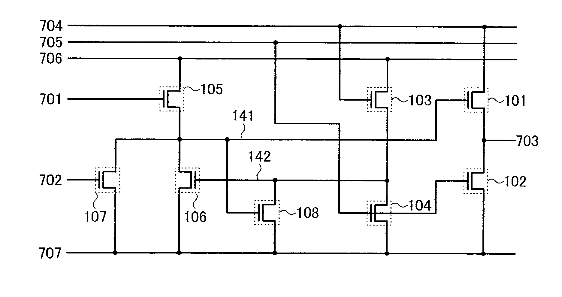
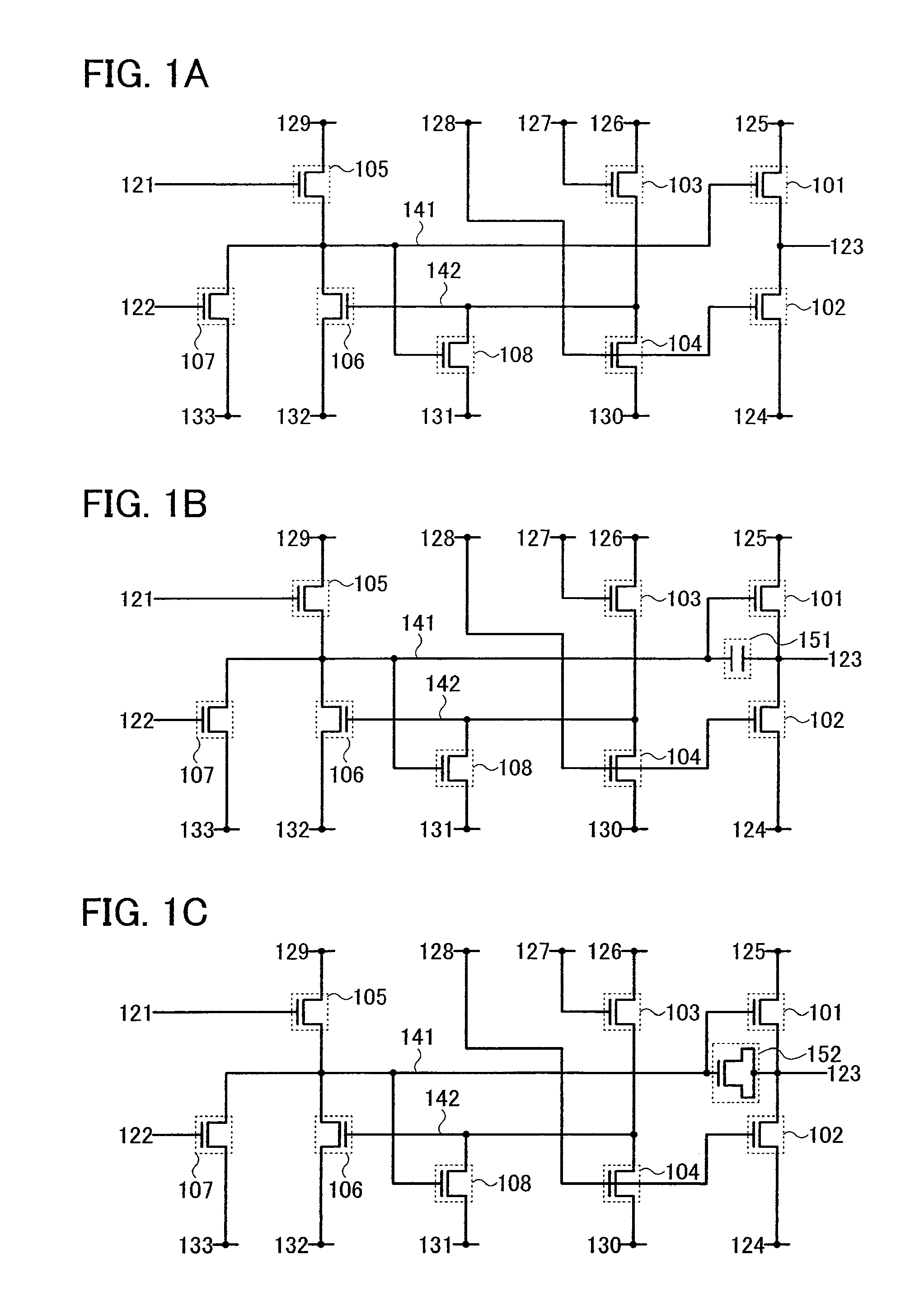
[0183]A basic structure of a flip-flop of this embodiment mode is described with reference to FIG. 1A. A flip-flop shown in FIG. 1A includes a first transistor 101, a second transistor 102, a third transistor 103, a fourth transistor 104, a fifth transistor 105, a sixth transistor 106, a seventh transistor 107, and an eighth transistor 108. In this embodiment mode, each of the first transistor 101, the second transistor 102, the third transistor 103, the fourth transistor 104, the fifth transistor 105, the sixth transistor 106, the seventh transistor 107, and the eighth transistor 108 is an N-channel transistor and is turned on when gate-source voltage (Vgs) exceeds the threshold voltage (Vth).

[0184]Note that in the flip-flop of this embodiment mode, the first transistor 101, the second transistor 102,...

embodiment mode 2

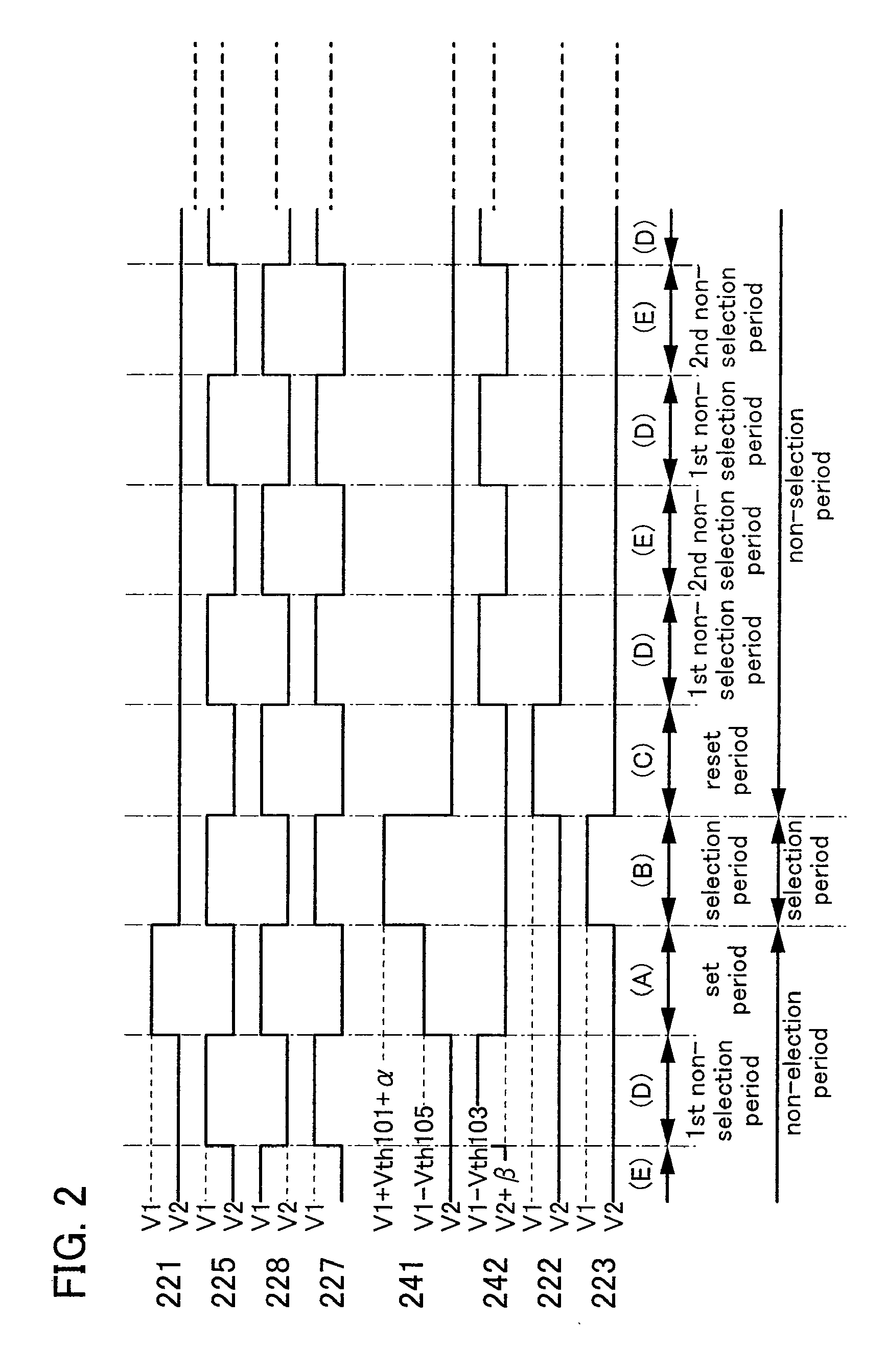
[0280]In this embodiment mode, structures and driving methods of a flip-flop which is different from those of Embodiment Mode 1, a driver circuit including the flip-flop, and a display device including the driver circuit are described. Note that portions which are similar to those of Embodiment Mode 1 are denoted by common reference numerals and detailed description of the portions which are the same and portions which have similar functions is omitted.

[0281]As a structure of the flip-flop of this embodiment mode, a structure which is similar to that of the flip-flop of Embodiment Mode 1 can be used. Note that drive timing of the flip-flop is different from that of Embodiment Mode 1. Thus, in this embodiment mode, description of the structure of the flip-flop is omitted.

[0282]Note that although the case is described in which the drive timing of this embodiment mode is applied to the flip-flop in FIG. 1A, the drive timing of this embodiment mode can be freely combined with each of th...

embodiment mode 3

[0310]In this embodiment mode, structures and driving methods of a flip-flop which is different from those of Embodiment Modes 1 and 2, a driver circuit including the flip-flop, and a display device including the driver circuit are described. In the flip-flop of this embodiment mode, an output signal of the flip-flop and a transfer signal of the flip-flop are output from different wirings by different transistors. Note that portions which are similar to those of Embodiment Modes 1 and 2 are denoted by common reference numerals and detailed description of the portions which are the same and portions which have similar functions is omitted.

[0311]A basic structure of the flip-flop of this embodiment mode is described with reference to FIG. 40. A flip-flop shown in FIG. 40 is similar to the flip-flop in FIG. 1A to which a ninth transistor 109 and a tenth transistor 110 are added.

[0312]Connection relations of the flip-flop in FIG. 40 are described. A first electrode of the ninth transist...


PUM


Abstract

To suppress fluctuation in the threshold voltage of a transistor, to reduce the number of connections of a display panel and a driver IC, to achieve reduction in power consumption of a display device, and to achieve increase in size and high definition of the display device. A gate electrode of a transistor which easily deteriorates is connected to a wiring to which a high potential is supplied through a first switching transistor and a wiring to which a low potential is supplied through a second switching transistor; a clock signal is input to a gate electrode of the first switching transistor; and an inverted clock signal is input to a gate electrode of the second switching transistor. Thus, the high potential and the low potential are alternately applied to the gate electrode of the transistor which easily deteriorates.

Description

BACKGROUND OF THE INVENTION[0001]1. Field of the Invention[0002]The present invention relates to a display device including a circuit formed by using a transistor. In particular, the present invention relates to a display device using an electro-optical element such as a liquid crystal element, a light-emitting element, or the like as a display medium, and an operating method thereof.[0003]2. Description of the Related Art[0004]In recent years, with the increase of large display devices such as liquid crystal televisions, display devices have been actively developed. In particular, a technique for forming a pixel circuit and a driver circuit including a shift register or the like (hereinafter also referred to as an internal circuit) over the same insulating substrate by using transistors formed of a non-crystalline semiconductor (hereinafter also referred to as amorphous silicon) has been actively developed, because the technique greatly contributes to low power consumption and low ...

Claims


Application Information

Patent Timeline
Patent Type & Authority Patents(United States)
IPC IPC(8): G09G3/36
CPCG09G3/3677G11C19/28G09G2310/0205G09G2310/061G09G2310/0248A01K97/10Y10S81/01H01L27/1222H01L27/1225G09G3/2092G09G3/3266G09G3/3674G09G2300/0809G09G2310/0286G09G2310/0289G09G2310/0291G09G2320/0646G09G2320/0666H01L27/0207H01L27/124
Inventor UMEZAKI, ATSUSHIMIYAKE, HIROYUKI
Owner SEMICON ENERGY LAB CO LTD
Why Eureka
Try Eureka