Semiconductor thin film manufacturing method and device, beam-shaping mask, and thin film transistor

a technology of semiconductors and thin films, applied in the direction of polycrystalline material growth, crystal growth process, instruments, etc., can solve the problems of reduced mobility of carriers, grain boundaries, deterioration of carrier mobility, etc., and achieves high ion current, large transmittivity of laser light, and high mobility of carriers.

Active Publication Date: 2005-10-06
HANNSTAR DISPLAY CORPORATION
View PDF38 Cites 20 Cited by
  • Summary
  • Abstract
  • Description
  • Claims
  • Application Information

AI Technical Summary

Benefits of technology

[0038] With the present invention, it enables to achieve high-mobility of carrier and high ion current since the crystal grain boundaries are not contained in the active layer.
[0039] With the manufacturing method and the manufacturing device according to the present invention, it enables to decrease the number of the crystal grain boundaries in the semiconductor thin film and also to manufacture the semiconductor thin film in which the directions of the crystal grain boundaries are controlled. Further, the transmittivity of the laser light is larger compared to the case of the zigzag pattern so that the beam length can be extended and the one-time scanning irradiation region can be widened. Thereby, the time required for the laser annealing processing per substrate can be shortened. Further, by shortening the convex width of the beam in the concave pattern, the high-density grain boundary region generated in the irradiation start position can be narrowed compared to the case of the zigzag pattern. Furthermore, since the front-half end of the beam is a straight line towards the direction vertical to the scanning direction, the high-density grain boundary region generated in the irradiation end position becomes about the crystal growth distance achieved by one-time irradiation. Thus, it becomes narrower than the case of the zigzag pattern. Also, the step for manufacturing the mask for the concave pattern is easier compared to the case of the zigzag pattern and the manufacturing cost can be decreased. Furthermore, it does not require the high resolution as much in the optical system of the laser annealing device when forming the concave-pattern beam shape compared to the case of forming the zigzag-pattern beam shape. Moreover, the TFT manufactured using the obtained semiconductor thin film enables to improve the carrier mobility and to suppress the dispersions in the mobility and the threshold voltage.
[0040] Further, another object is to shorten the laser annealing processing time, to narrow the high-density grain boundary region generated in the start position and the end position of the irradiation, to decrease the cost for manufacturing the mask, and to achieve the low resolution of the optical system in the laser annealing device by improving the transmittivity of the optical system compared to the case of zigzag pattern. Still another object of the present invention is to improve the action speed of the TFTs manufactured using the obtained semiconductor thin film so as to suppress the dispersions in the action speeds and in the threshold voltages.

Problems solved by technology

However, when there are a large number of grain boundaries present within the channel, the mobility of the carrier is decreased.
As a result, when TFTs are manufactured by providing channels so that the carriers move in parallel to the scanning direction, there are crystal grain boundaries generated in the channels since the positions of the crystal grain boundaries are not controlled.
Thus, the mobility of carrier is deteriorated and fluctuations in the mobility and threshold voltage are increased.
Further, when the TFTs are manufactured by providing the channels so that the carriers move in the direction vertical to the scanning direction, there are crystal grain boundaries generated in the channels by interrupting the transition of the carriers since the positions of the crystal grain boundaries are not controlled.
Thus, the mobility of carrier is deteriorated and fluctuations in the mobility and threshold voltage are increased.
Also, in a step of manufacturing the mask, forming a complicated zigzag pattern increases the cost compared to the case of forming a straight-line pattern.

Method used


Image

  • Semiconductor thin film manufacturing method and device, beam-shaping mask, and thin film transistor
  • Semiconductor thin film manufacturing method and device, beam-shaping mask, and thin film transistor
  • Semiconductor thin film manufacturing method and device, beam-shaping mask, and thin film transistor

Examples


example 1

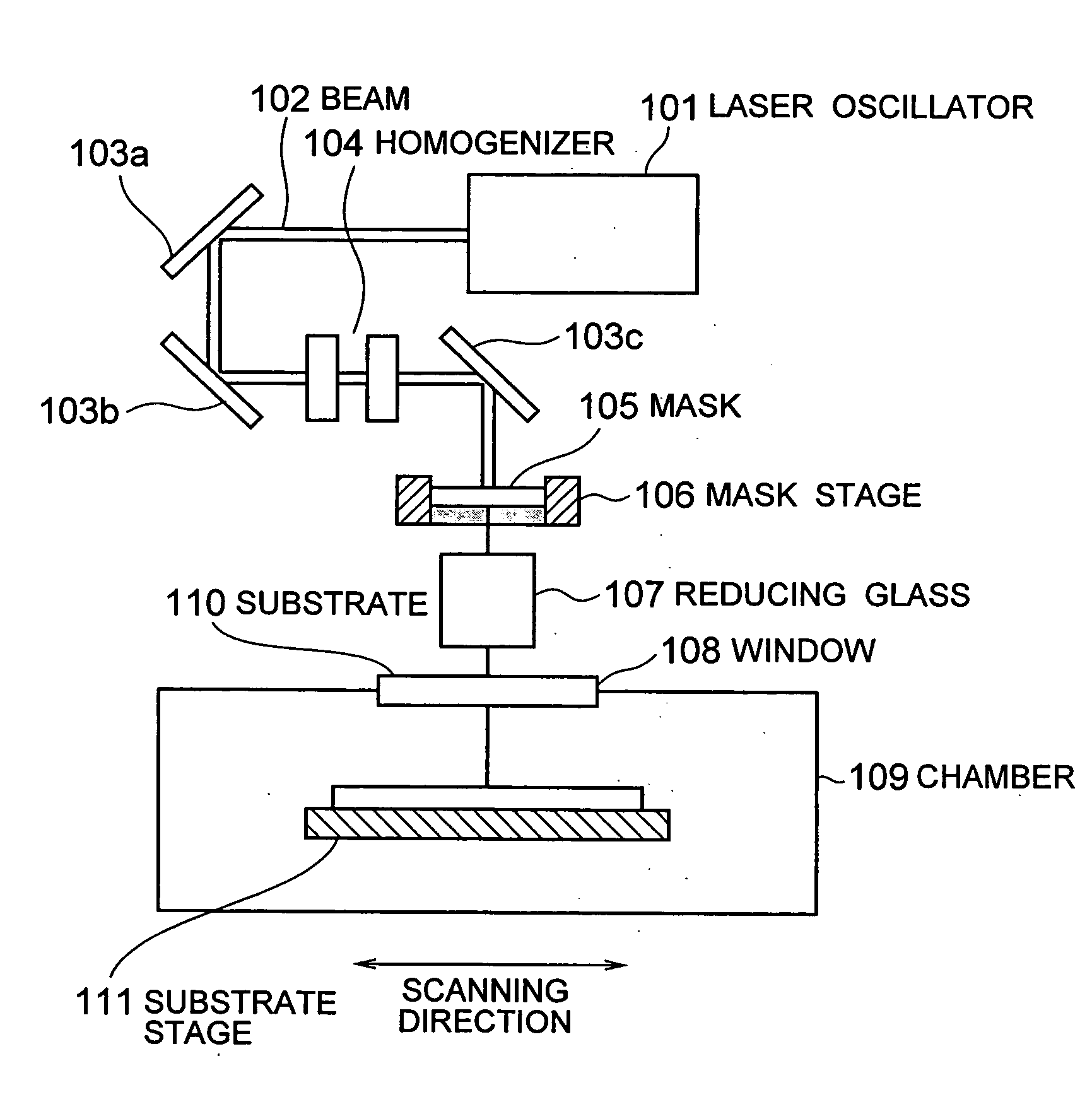
[0073] Laser annealing was performed using the laser annealing device shown in FIG. 4. The method, the mask, and the laser used therefore were the ones described in the embodiment. As for the openings and the transmission section formed in the mask, a large number of slots in an extremely narrow width may be formed in line to be the openings and the like, or a large number of pores may be collectively formed to be the openings and the like. In this case, by changing the number of the slits or the density of the pores, the energy of the laser light can be altered. The substrate will be described. A no alkali glass was used for the glass substrate. On the glass substrate, an insulating film for preventing diffusion of impurities from the glass was formed. On the insulating film, an amorphous silicon film of 60 nm as the precursor film was formed by low pressure chemical vapor deposition (LP-CVD).

[0074] In this EXAMPLE, scanning irradiation was performed by using the mask in a shape s...

example 2

[0076] By using the same laser annealing device as that of EXAMPLE 1 and the mask in the shape shown in FIG. 7(1), scanning irradiation was performed by changing the beam concave length from 1.5 μm, 3 μm, 6 μm and to 12 μm. The irradiation condition is shown in TABLE 2. The irradiation intensity is the value on the substrate. The step width is the distance on the substrate scanned between each irradiation. The opening width 402, the concave length 404, and the concave width 403 in the TABLE are the values on the mask. The beam passed through the mask becomes in the shape shown in FIG. 7(2) on the substrate. The beam size on the substrate becomes the ⅓ of the beam size on the mask. That is, the beam width 502 is 10 μm, the beam concave length 504 is 0.5 μm, 1 μm, 2 μm, or 4 μm, and the beam concave width 503 is 5 μm.

TABLE 2EXAMPLE2-12-22-32-4Irradiation intensity (mJ / cm2)600600600600Step width (μm)0.50.50.50.5Opening width (μm)30303030Concave length (μm)1.53612Concave width (μm)151...

example 3

[0083] Scanning irradiation was performed by using the same laser annealing device as that of EXAMPLE 1 and the mask in the shape as shown in FIG. 5(1) in which the concave patterns 306c were periodically formed. The irradiation condition is shown in TABLE 3. The irradiation intensity is the value on the substrate. The step width is the distance on the substrate scanned between each irradiation. The opening width 203, the concave length 202, the concave width 204, and the convex length 205 in the TABLE are the values on the mask. The beam passed through the mask becomes in the shape shown in FIG. 5(2) on the substrate. The beam size on the substrate becomes the ⅓ of the beam size on the mask. That is, the beam width 303 is 6 μm, the beam concave length 302 is 1 μm, the beam concave width 304 is 3 μm, and the beam convex length 305 is 1 μm.

TABLE 3EXAMPLE 3Irradiation intensity (mJ / cm2)600Step width (μm)0.2Opening width (μm)18Concave length (μm)3Concave width (μm)9Convex length (μm)...


PUM

PropertyMeasurementUnit
wavelengthaaaaaaaaaa
crystal growth widthaaaaaaaaaa
lengthaaaaaaaaaa

Abstract

A manufacturing method of a semiconductor thin film decreases the number of and controls the direction of crystal grain boundaries. A first beam irradiated onto amorphous silicon produces a radial temperature gradient centered on a tip of a concave. This forms a crystal grain in the concave tip, which grows in both the beam width and length direction. After the second beam and on, growth is repeated using the crystal grain formed in the tip of the concave as the seed. This forms a band-form crystal grain with a wider than that of the conventional narrow-line beam, with the tip of the concave being the start point. Further, by setting the periphery of the concave pattern to be equal or less than the crystal grain diameter in the direction vertical to the beam scanning direction, it is possible to form the band-form crystal grain being lined continuously.

Description

BACKGROUND OF THE INVENTION [0001] 1. Field of the Invention [0002] The present invention relates to a method and a device for manufacturing a semiconductor thin film especially with controlled grain boundaries and to a thin film transistor. [0003] 2. Description of the Related Art [0004] As a switching device for constituting pixels in a liquid crystal display device, used is a thin film transistor (referred to as a “TFT” hereinafter) formed on a glass substrate. Recently, in addition to achieving highly fine liquid crystal display devices, there has been an increasing demand for improving the action speed of the TFTs in order to achieve a system-on-glass, and a technique for forming a high-quality laser annealed polycrystalline silicon TFT has drawn an attention. [0005] The above-described TFT is manufactured in the manner as shown in FIG. 1. For example, as shown in FIG. 1(1), amorphous silicon 1201 is formed on an insulating film 1202 which is formed on a surface of a glass subs...

Claims


Application Information

Patent Timeline
Patent Type & Authority Applications(United States)
IPC IPC(8): H01L21/20H01L21/84H01L21/027G02F1/136H01L21/336H01L29/786
CPCH01L29/66757H01L29/78675Y10S117/904Y10S438/942
Inventor NAKATA, MITSURU
Owner HANNSTAR DISPLAY CORPORATION
Why Eureka
Try Eureka