
Process variation compensated multi-chip memory package

a multi-chip memory and process variation technology, applied in the field of multi-chip memory packages, can solve the problem that the vertical connection paths formed by multiple vertical connection elements are inherently susceptible to process, and achieve the effect of reducing power consumption

Active Publication Date: 2011-11-08
SAMSUNG ELECTRONICS CO LTD
View PDF20 Cites 19 Cited by
  • Summary
  • Abstract
  • Description
  • Claims
  • Application Information

AI Technical Summary

Benefits of technology

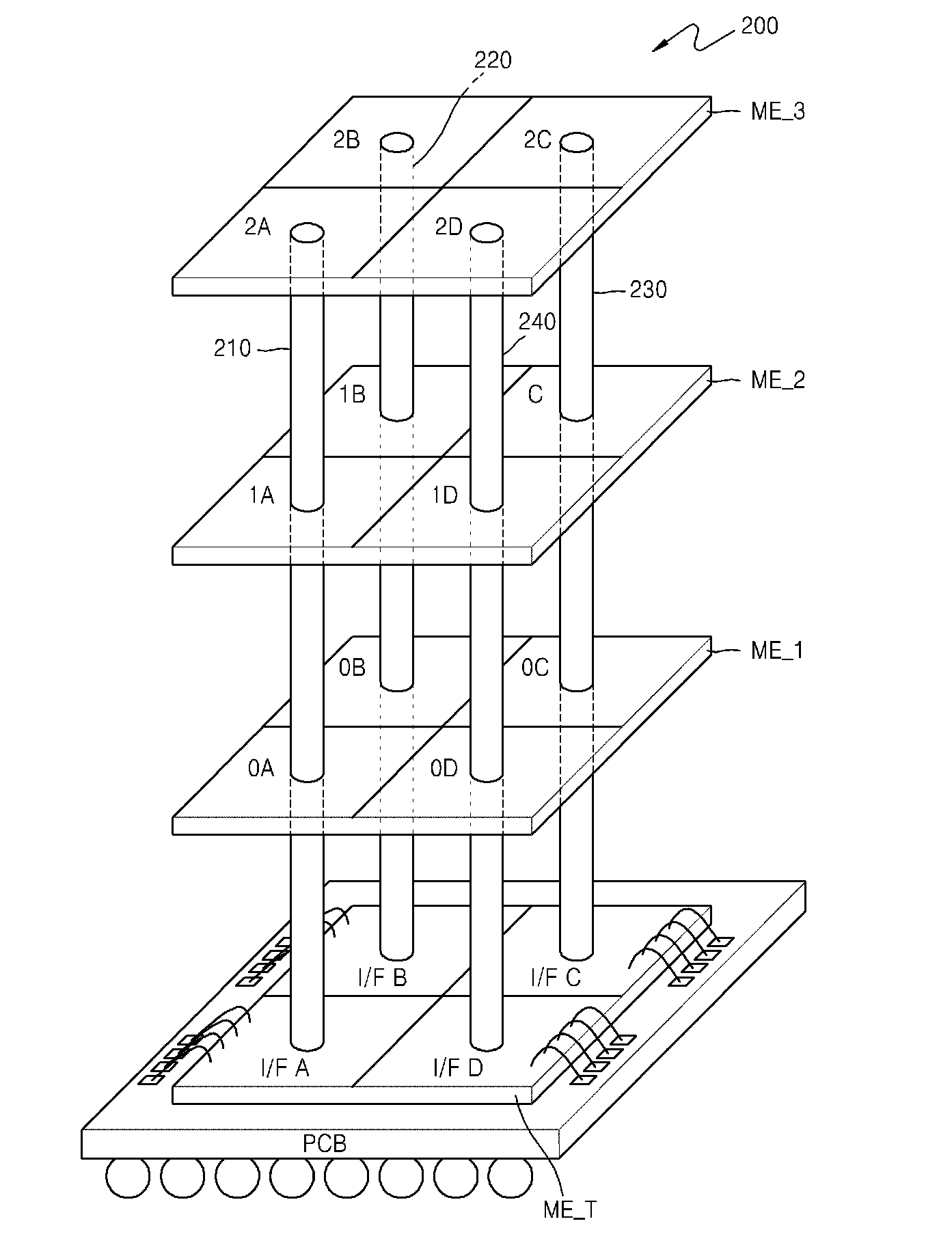
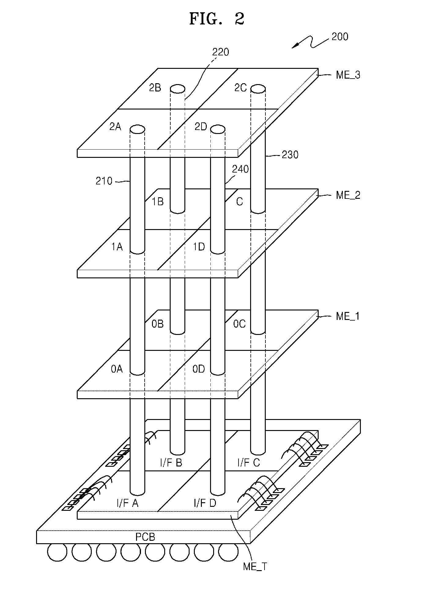
[0008]Embodiments of the invention provide a multi-chip package memory which compensates for process variations influencing the performance of stacked memory chips in order to prevent malfunctions and reduce power consumption.

Problems solved by technology

Unfortunately, stack connection approaches relying on vertical connection paths formed by multiple vertical connection elements are inherently susceptible to process variations in the manufacture of individual memory chips and related packaging processes.

Method used


Image

  • Process variation compensated multi-chip memory package
  • Process variation compensated multi-chip memory package
  • Process variation compensated multi-chip memory package

Examples


Embodiment Construction

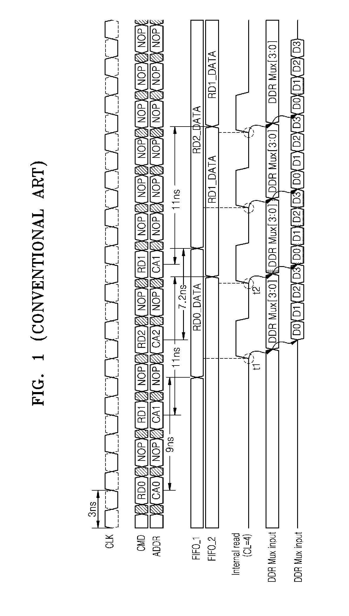
[0019]The difficulties noted above in relation to conventional multi-chip package memories and related process variations are further illustrated by way of background information in relation to FIG. 1. FIG. 1 is a signal and data waveform diagram characterizing a read operation executed in accordance with a technique associated with a conventional multi-chip package memory that receives an externally provided clock CLK.

[0020]Within FIG. 1, a first read command RD0 is applied to a first memory chip within a stacked plurality of memory chips as a CMD command signal, a second read command RD1 is applied to a second memory chip, and a third read command RD2 is applied to a third memory chip. No operation performed NOP commands are also shown in between the read (RD) commands. Taking into account all relevant process variations, the first memory chip outputs read data in 9 ns. That is, a first time interval between receipt (input) of the first read command RD0 and provision (output) of t...


PUM


Abstract

A multi-chip package memory includes an interface chip generating at least one reference signal defined in relation to a reference process variation, and a stacked plurality of memory chips electrically connected to the interface chip via a vertical connection path and receiving the reference clock signal via the vertical connection path, wherein each one of the stacked plurality of memory chips is characterized by a process variation and actively compensates for said process variation in relation to the reference signal.

Description

CROSS-REFERENCE TO RELATED PATENT APPLICATIONS[0001]This application claims the benefit of Korean Patent Application No. 10-2008-0025377 filed on Mar. 19, 2008, the subject matter of which is hereby incorporated by reference.BACKGROUND OF THE INVENTION[0002]The present invention relates generally to multi-chip memory packages and methods of fabricating same. More particularly, the invention is related to multi-chip memory packages in which fabrication process variations are compensated.[0003]As the size of mobile electronic devices decreases, the packaged semiconductor memories incorporated within these devices must be fabricated with ever more compact and lightweight designs. Reductions in size, weight and current consumption notwithstanding, semiconductor memories must operate at high speed with increased bandwidth. As a result, legacy electronic mobile devices included single-chip package memories. More recently, electronic mobile devices include multi-chip package memories forme...

Claims


Application Information

Patent Timeline
Patent Type & Authority Patents(United States)
IPC IPC(8): G11C5/02G11C7/00G11C8/00
CPCG11C5/02G11C5/063H01L25/0657H01L2225/06527H01L2225/06541H01L2224/48091H01L2224/48227H01L2924/15311H01L2924/00014G11C5/06
Inventor CHUNG, HOE-JU
Owner SAMSUNG ELECTRONICS CO LTD
Learn More