Multiple-gate transistors with reverse T-shaped fins

a multi-gate transistor and reverse t-shaped technology, applied in the direction of transistors, semiconductor devices, electrical apparatus, etc., can solve the problems of difficult to form germanium films with high germanium concentrations or pure germanium films, difficult gate dielectric formation, and oxidation of germanium, so as to reduce defects in germanium films, high drive current of finfets, and high germanium percentage

Active Publication Date: 2011-11-15
TAIWAN SEMICON MFG CO LTD
View PDF21 Cites 32 Cited by
  • Summary
  • Abstract
  • Description
  • Claims
  • Application Information

AI Technical Summary

Benefits of technology

[0007]The advantageous features of the present invention include high drive currents of FinFETs due to the fact that the resulting FinFETs may have high germanium percentages and reduced defects in germanium films. Further, the pitches for forming STI regions, which are used for forming germanium-containing fins, are also relaxed.

Problems solved by technology

The oxide of germanium, on the other hand, is soluble in water, and hence is not suitable for the formation of gate dielectrics.
A challenge faced by the semiconductor industry is that it is difficult to form germanium films with high germanium concentrations or pure germanium films.
Particularly, it is difficult to form high-concentration germanium films with low defect densities and great thicknesses, which germanium films are required for forming FinFETs.
For example, when formed on blanket silicon wafers, the critical thickness of a silicon germanium film having a 20% germanium percentage may be about 10 nm to about 20 nm, which thickness is still not adequate for forming FinFETs.
Accordingly, it is not feasible to form germanium films on blanket silicon wafers for the purpose of forming FinFETs.

Method used


Image

  • Multiple-gate transistors with reverse T-shaped fins
  • Multiple-gate transistors with reverse T-shaped fins
  • Multiple-gate transistors with reverse T-shaped fins

Examples


Embodiment Construction

[0010]The making and using of the embodiments of the present invention are discussed in detail below. It should be appreciated, however, that the present invention provides many applicable inventive concepts that can be embodied in a wide variety of specific contexts. The specific embodiments discussed are merely illustrative of specific ways to make and use the invention and do not limit the scope of the invention.

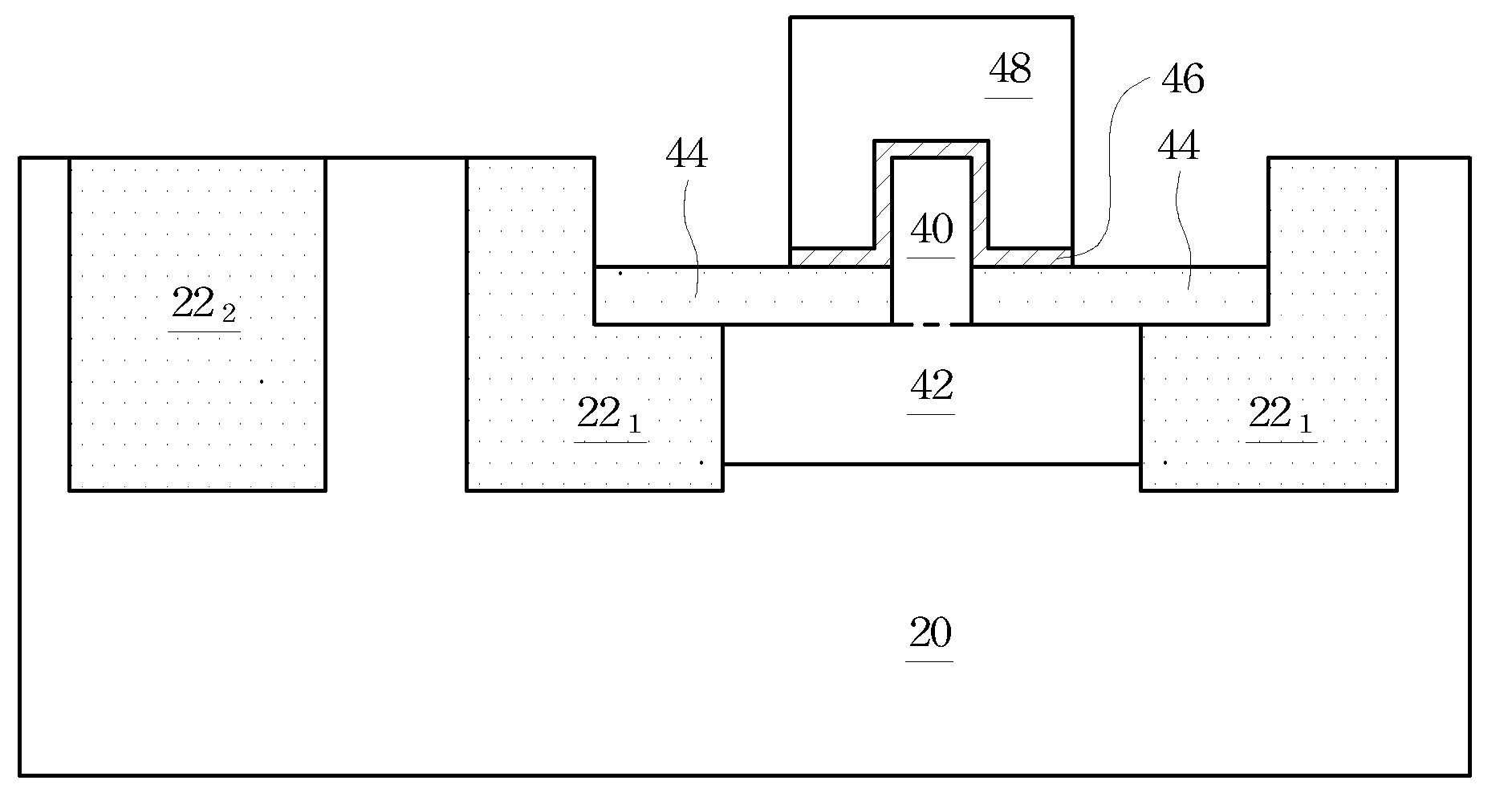
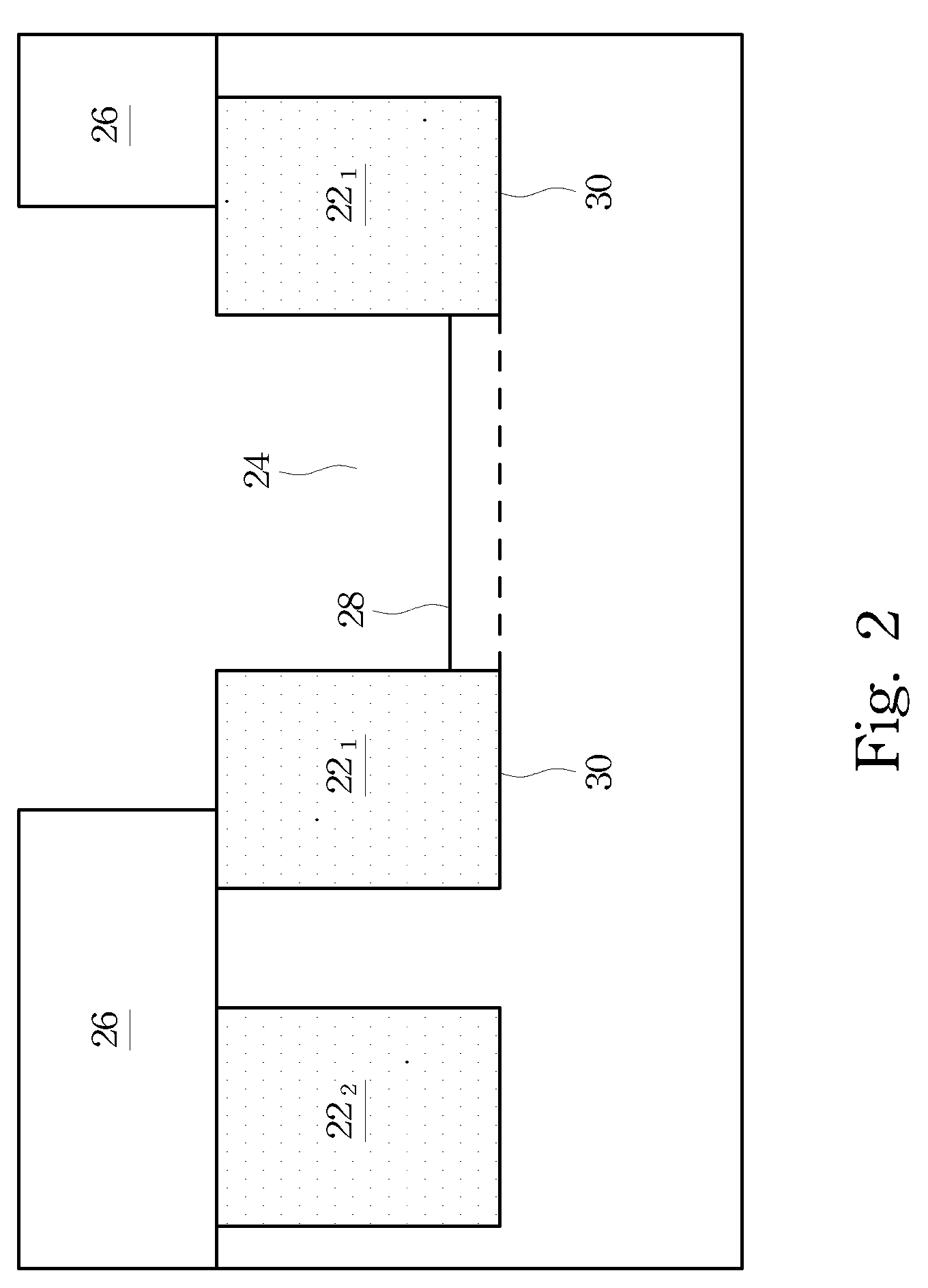
[0011]An integrated circuit formation process including the formation of a germanium region having a reversed T-shape, which may be used to form a fin field-effect transistor (FinFET) (also referred to as a multi-gate transistor), is provided. The intermediate stages of manufacturing an embodiment of the present invention are illustrated. The variations of the embodiment are discussed. Throughout the various views and illustrative embodiments of the present invention, like reference numbers are used to designate like elements.

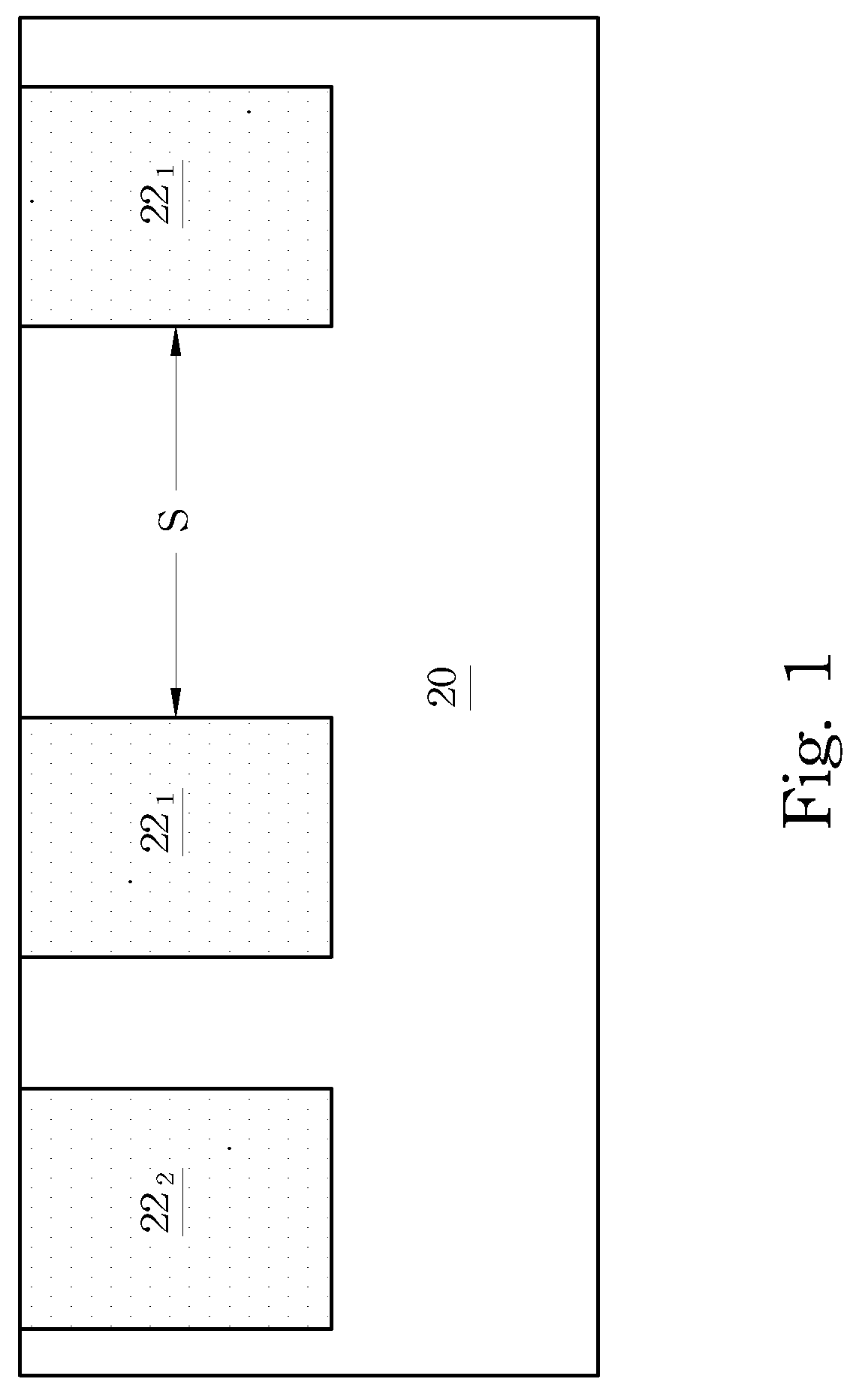
[0012]Referring to FIG. 1, semiconductor subst...


PUM


Abstract

A method of forming an integrated circuit structure includes forming a first insulation region and a second insulation region in a semiconductor substrate and facing each other; and forming an epitaxial semiconductor region having a reversed T-shape. The epitaxial semiconductor region includes a horizontal plate including a bottom portion between and adjoining the first insulation region and the second insulation region, and a fin over and adjoining the horizontal plate. The bottom of the horizontal plate contacts the semiconductor substrate. The method further includes forming a gate dielectric on a top surface and at least top portions of sidewalls of the fin; and forming a gate electrode over the gate dielectric.

Description

TECHNICAL FIELD[0001]This invention relates generally to semiconductor devices, and particularly to structures and formation methods of Fin field-effect transistors (FinFET) having germanium-containing fins.BACKGROUND[0002]Fin field-effect transistors (FinFET) are promising devices in small-scale integrated circuits, such as 22 nm technology and below, for their high drive currents and low chip-area usage. To further improve the drive currents of FinFETs, semiconductor materials having high electron mobility and hole mobility may be used in FinFET structures.[0003]Germanium is a commonly known semiconductor material. The electron mobility and hole mobility of germanium are greater than that of silicon, hence making germanium an excellent material in the formation of integrated circuits. However, in the past, silicon gained more popularity since its oxide (silicon oxide) is readily usable in the gate dielectric of metal-oxide-semiconductor (MOS) transistors. The gate dielectrics of t...

Claims


Application Information

Patent Timeline
Patent Type & Authority Patents(United States)
IPC IPC(8): H01L29/786
CPCH01L29/66795H01L29/785H01L29/1054H01L29/165H01L29/768
Inventor LAI, LI-SHYUELIN, JING-CHENG
Owner TAIWAN SEMICON MFG CO LTD
Why Eureka
Try Eureka