
Solid state image sensing device

a sensing device and solid state technology, applied in the field of solid state image sensing devices, can solve the problems of difficult to reduce the time required for performing the operation (2) of performing a/d conversion, and achieve the effects of high-precision a/d conversion, reduced horizontal scanning period, and increased frame ra

Inactive Publication Date: 2011-12-06
KONICA MINOLTA BUSINESS TECH INC
View PDF8 Cites 6 Cited by
  • Summary
  • Abstract
  • Description
  • Claims
  • Application Information

AI Technical Summary

Benefits of technology

This approach enables high-precision A / D conversion while reducing the horizontal scanning period, thereby enhancing the frame rate and achieving high-speed photographing capabilities.

Problems solved by technology

It is, however, difficult to reduce the time required for performing the operation (2) of performing A / D conversion with respect to data of upper two bits.

Method used


Image

  • Solid state image sensing device
  • Solid state image sensing device
  • Solid state image sensing device

Examples


first embodiment

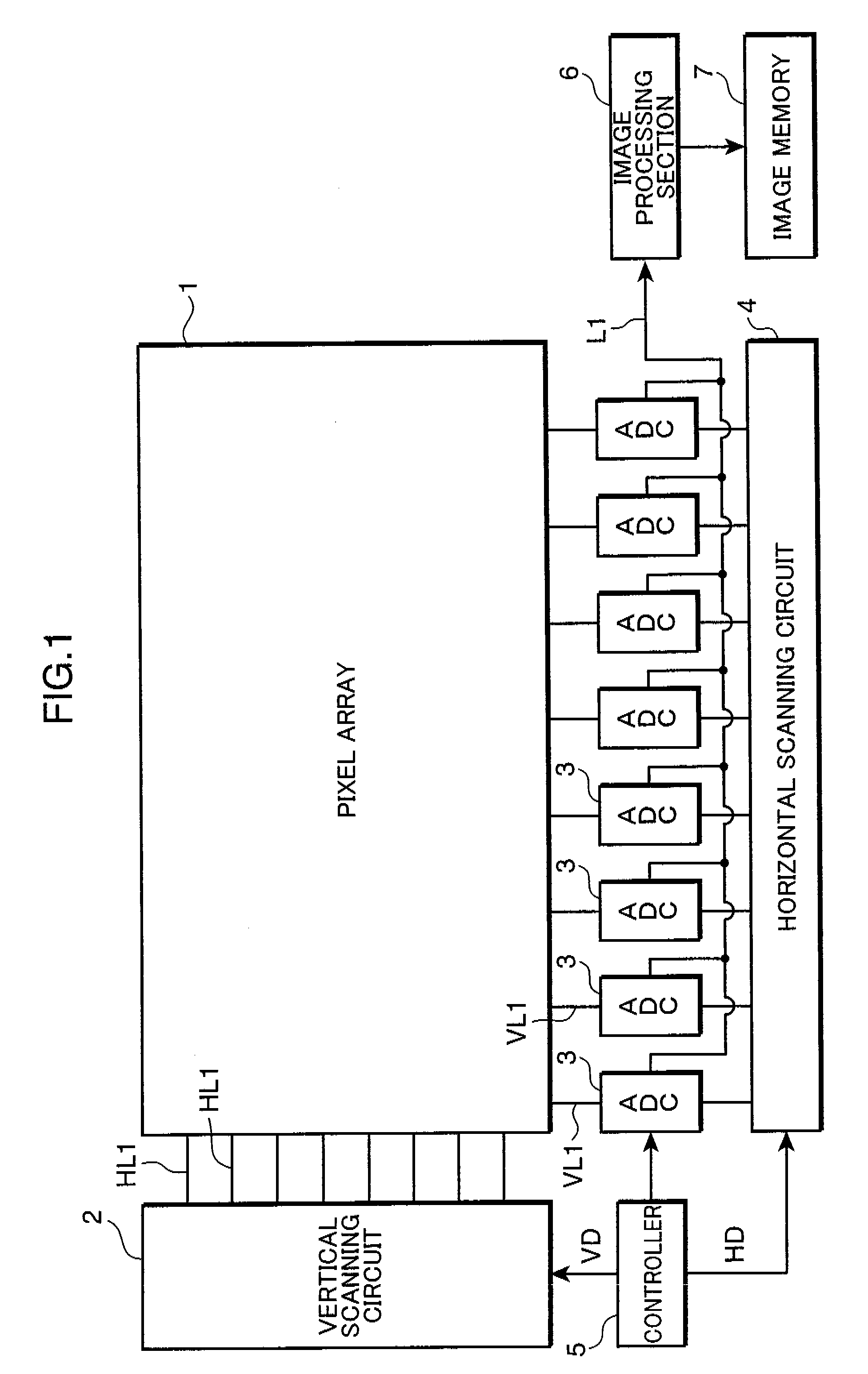
FIG. 1 is a diagram schematically showing the entire arrangement of a solid state image sensing device in accordance with the first embodiment of the invention. As shown in FIG. 1, the solid state image sensing device is a solid state image sensing device incorporated with a CMOS image sensor provided with a column A / D converter; and includes a pixel array 1, a vertical scanning circuit 2, column A / D converters (or ADC) 3, a horizontal scanning circuit 4, a controller 5, an image processing section 6, and an image memory 7.

The pixel array 1 is constituted of multiple pixels arranged in a matrix of eight rows and eight columns. The pixel array 1 constituted of pixels arranged in eight rows and eight columns is merely an example, and may be constituted of pixels arranged in M (where M is an integer of 2 or more) rows and N (where N is an integer of 2 or more) columns.

The vertical scanning circuit 2 includes e.g. a shift register, and is connected to the pixel array 1 via eight pixel c...

second embodiment

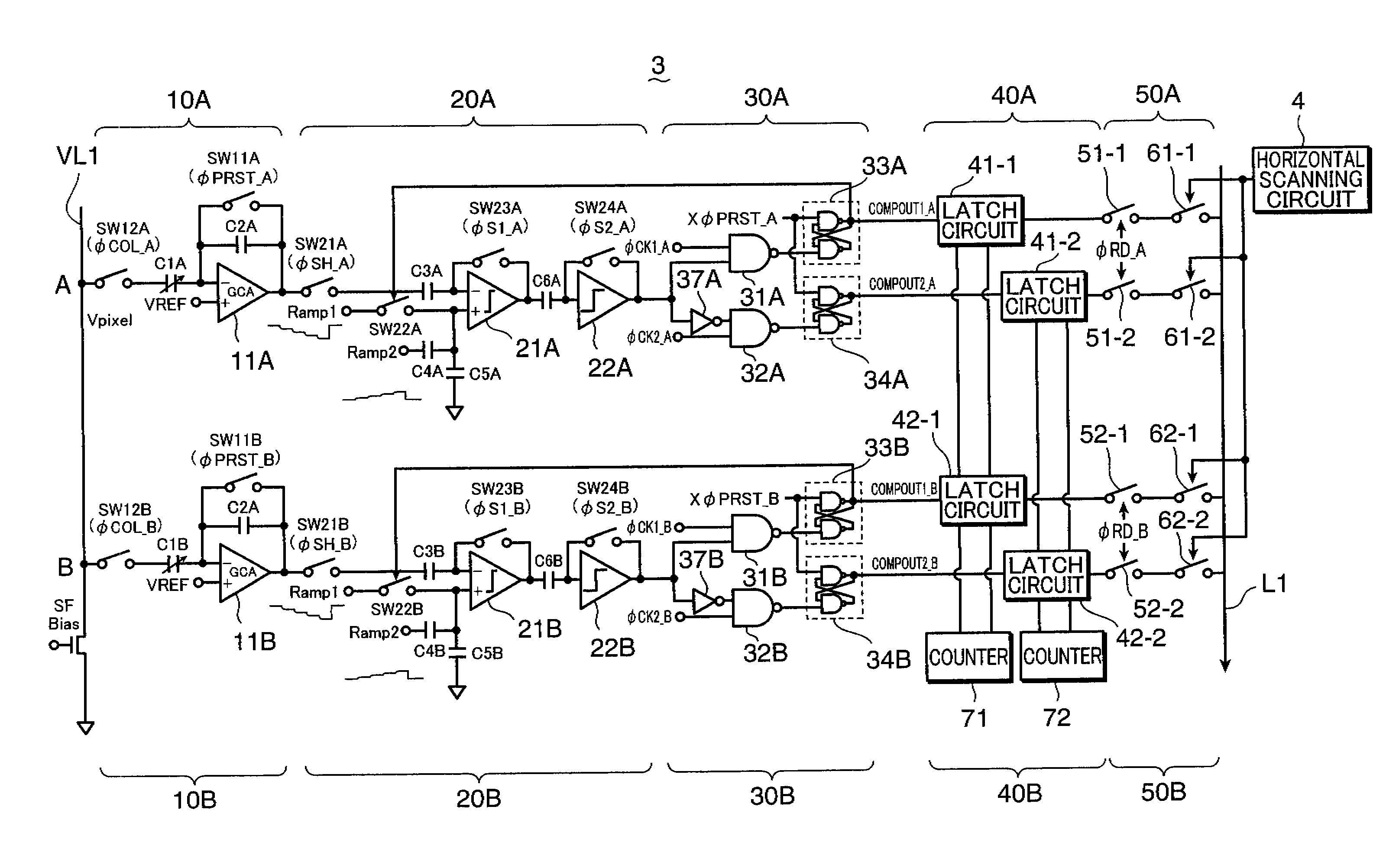
In this section, a solid state image sensing device in accordance with the second embodiment of the invention is described. The solid state image sensing device in accordance with the second embodiment has a feature that latch circuits 41-1 and 41-2, and a GCA section 10A are used in common between column A / D converting elements “A” and “B”. Elements in the second embodiment substantially identical or equivalent to those in the first embodiment are indicated with the same reference numerals, and description thereof is omitted herein.

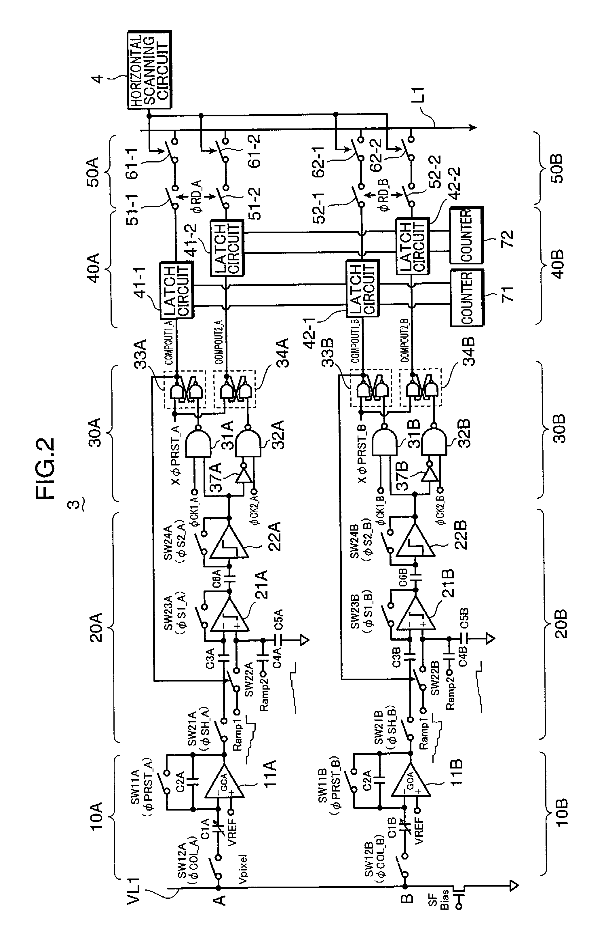
FIG. 6 is a circuit diagram of a column A / D converter 3 in the second embodiment of the invention. The GCA section 10A has an output portion connected to a comparator section 20A and a comparator section 20B, and is used in common between the column A / D converting elements “A” and “B”.

A latch section 40A is connected to an output portion of a logic circuit 30A and an output portion of a logic circuit 30B via a switch section 80A, and is used in common be...


PUM


Abstract

A column A / D converter includes two column A / D converting elements. Each of the column A / D converting elements is operable to divide a pixel signal read out from a pixel array into two blocks i.e. an upper block constituted of upper two bit data, and a lower block constituted of lower two bit data, and sequentially perform A / D conversion with respect to the blocks in the unit of one horizontal scanning period. A controller causes each of the column A / D converting elements to concurrently perform A / D conversion with respect to different blocks of pixel signals at different rows.

Description

This application is based on Japanese Patent Application No. 2008-163007 filed on Jun. 23, 2008, the contents of which are hereby incorporated by reference.BACKGROUND OF THE INVENTION AND RELATED ART STATEMENT1. Field of the InventionThe present invention relates to a solid state image sensing device provided with a column AD converter.2. Description of the Related ArtIn recent years, a solid state image sensing device incorporated with a CMOS (Complementary Metal Oxide Semiconductor) image sensor provided with a column A / D converter has been widely spread. For instance, there is known a solid state image sensing device including a pixel array constituted of pixels arranged in a matrix of a predetermined number of rows and a predetermined number of columns; and column A / D converting circuits corresponding to the columns of the pixel array, and for reading out a pixel signal from the pixel array for A / D conversion. Each of the column A / D converting circuits is a double integral A / D c...

Claims


Application Information

Patent Timeline
Patent Type & Authority Patents(United States)
IPC IPC(8): H04N5/335H04N25/00
CPCH04N5/374H04N5/378H04N25/76H04N25/78H04N25/75
Inventor KUSUDA, MASAYUKI
Owner KONICA MINOLTA BUSINESS TECH INC
Learn More