Semiconductor memory device

a memory device and semiconductor technology, applied in semiconductor devices, digital storage, instruments, etc., can solve the problems of lowering the supply voltage, unnecessary writing, and affecting the operation of the device, and achieve the effect of high operational reliability

Inactive Publication Date: 2011-12-06
KK TOSHIBA
View PDF5 Cites 20 Cited by
  • Summary
  • Abstract
  • Description
  • Claims
  • Application Information

AI Technical Summary

Benefits of technology

[0012]An object of the present invention is to provide a small-sized semiconductor memory device having high operational reliability.
[0014]According to the present invention, a small-sized semiconductor memory device having high operational reliability can be provided.

Problems solved by technology

Therefore, when a weak voltage is applied from a bit line due to noise and the like, erroneous write to the memory cell occurs due to the weak voltage.
Accordingly, when the SNM is low, unnecessary writing occurs due to noise and the like transferred from the bit line.
In consequence, the SRAMs formed with a configuration known in the prior art have problems associated with lowering of the supply voltage and reduction of the transistor size.
Thereby, the threshold voltage of the transfer transistor of a non-selected memory cell in which the back gate of the transfer transistor is at an “L” level is high enough to make it difficult to bring the transfer transistor of the non-selected memory cell into conduction.
On the other hand, this method has a problem that a reading speed and a writing speed are slow since a threshold voltage in the transfer gate of a selected memory cell is also high.
Consequently, in the prior art, it is difficult to provide a small-sized semiconductor memory device having high operational reliability.

Method used


Image

  • Semiconductor memory device
  • Semiconductor memory device
  • Semiconductor memory device

Examples


first embodiment

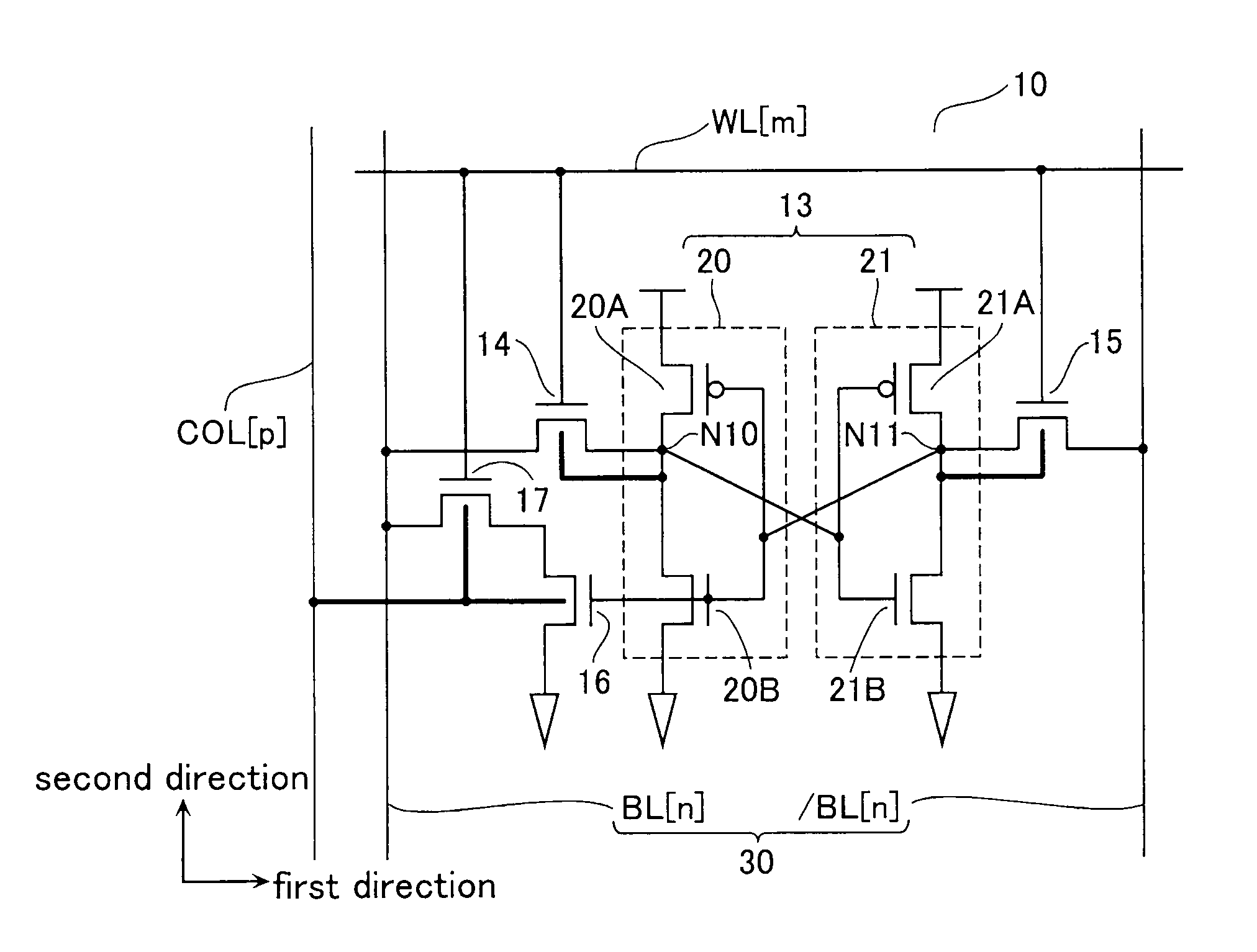
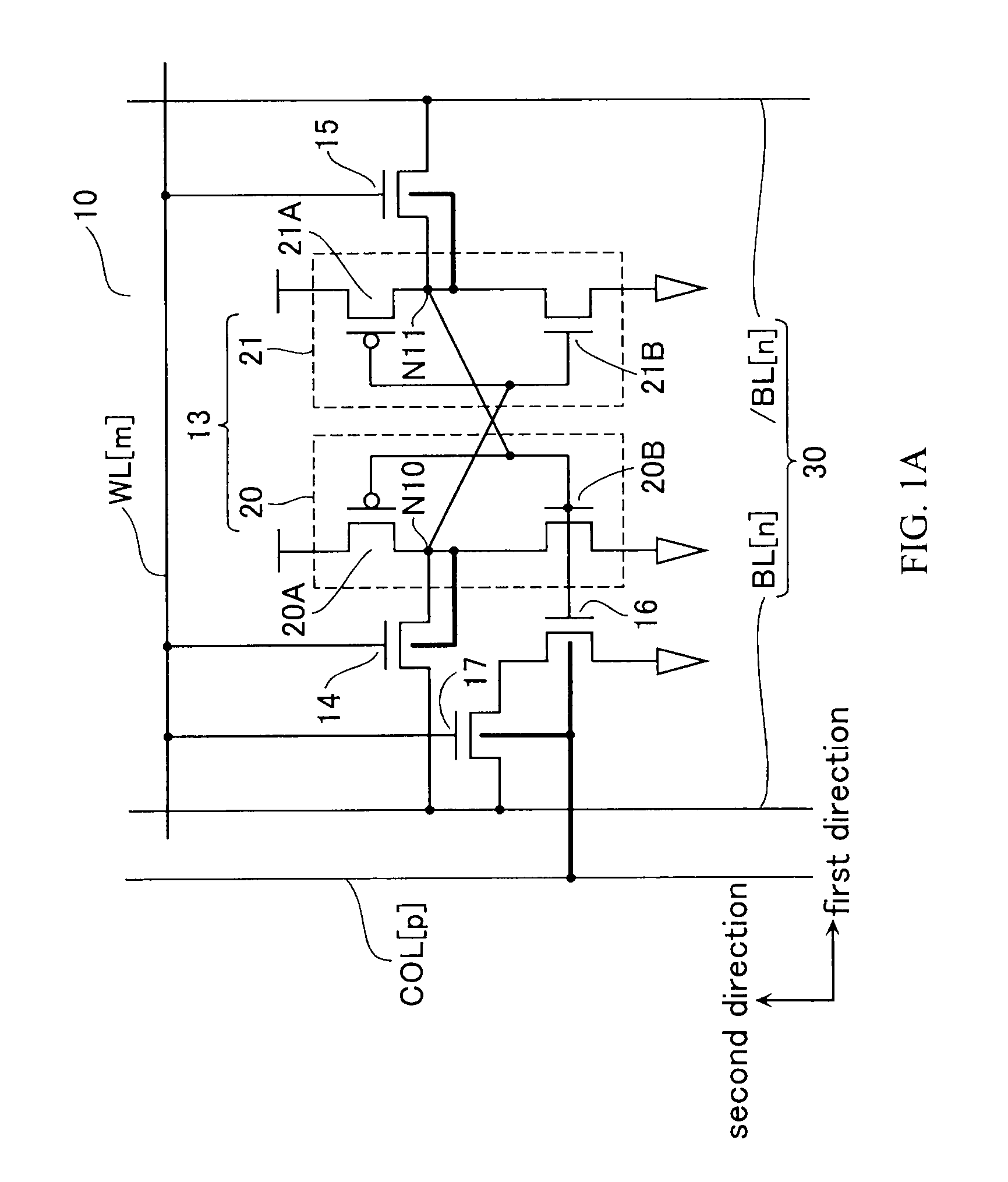
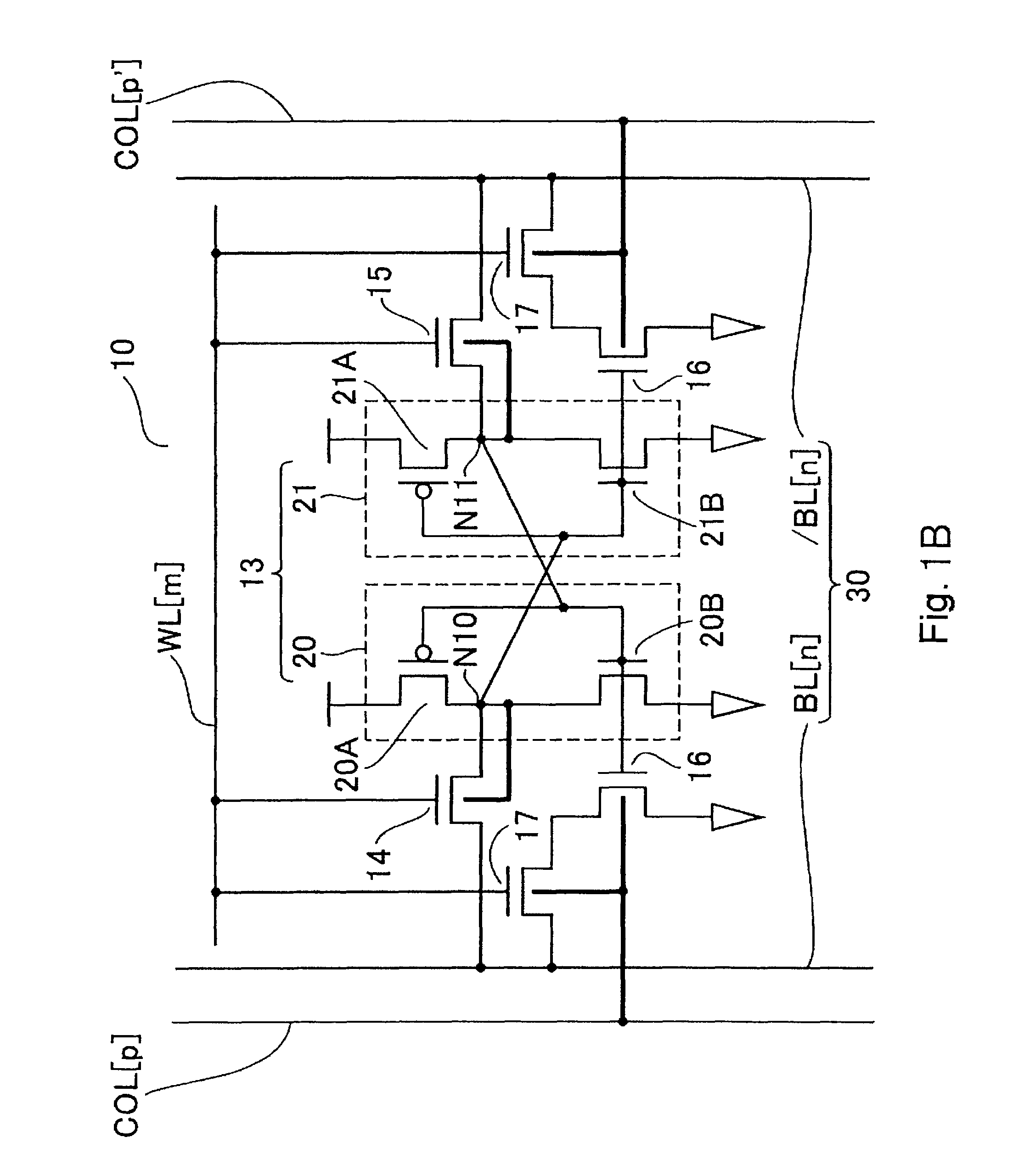
[0035]FIG. 1A is an equivalent circuit diagram showing a part of a semiconductor memory device (hereinafter, SRAM) 10 according to a first embodiment of the present invention. Memory cells MC constituting the SRAM 10 according to the first embodiment are formed at intersections of a plurality of word lines WL arranged in a first direction and a plurality of bit lines BL arranged in a second direction. For convenience in description, FIG. 1A shows a memory cell MC formed at an intersection of a word line WL[m] and a pair of bit lines BL[n] and / BL[n] (where m and n are natural numbers).

[0036]The memory cell MC is formed between a bit line pair 30 consisting of the bit line BL[n] and the bit line / BL[n], and includes a data storage unit 13 formed by cross-coupling an inverter 20 to an inverter 21. The inverter 20 is formed by connecting a pMOS transistor 20A and an nMOS transistor 20B in series. The inverter 21 is formed by connecting a pMOS transistor 21A and an nMOS transistor 21B i...

second embodiment

[0090]FIG. 6A is an equivalent circuit diagram showing a part of an SRAM 10 according to a second embodiment of the present invention. As shown in FIG. 6A, the second embodiment has a configuration in which instead of the word line WL[m] and the bit line BL[n] in the first embodiment, two word lines WL[m] and two bit lines BL[n] are provided for writing and reading. Only this point is different from the first embodiment, and the other points are the same as those in the first embodiment. In FIG. 6A, the same reference numerals are given to the same portions as those in the first embodiment and the detailed description thereof will be omitted below.

[0091]Each of memory cells MC that constitute the SRAM 10 according to the second embodiment is formed at an intersection of a write word line WWL and a read word line RWL which are arranged in a first direction, and write bit lines WBL and a read bit line RBL which are arranged in a second direction. For convenience in description, FIG. 6...

third embodiment

[0130]FIG. 9 is an equivalent circuit diagram showing a part of the SRAM 10 according to a third embodiment of the present invention. Unlike the first embodiment, the third embodiment has no column selection line COL, as shown in FIG. 9. Moreover, a third embodiment has a configuration in which a back gate of a read transistor 17 is connected to a node N11, and a driver transistor 16 is formed of a single gate FinFET. Only these points are different from those in the first embodiment, and the other points are the same as those in the first embodiment. In FIG. 9, the same reference numerals are given to the same portions as those in the first embodiment, and the detailed description will be omitted below.

[0131]Memory cells MC that constitute the SRAM 10 according to the third embodiment are formed at intersections of a plurality of word lines WL arranged in a first direction and a plurality of bit lines BL arranged in a second direction. For convenience in description, FIG. 9 shows a...


PUM


Abstract

The semiconductor memory device includes: an inverter pair of a cross-coupled first and second inverters; a first transfer transistor including a front gate and a back gate connected to a first node to which an output terminal of the first inverter and an input terminal of the second inverter are connected; a second transfer transistor including a front gate and a back gate connected to a second node to which an output terminal of the second inverter and an input terminal of the first inverter are connected; a driver transistor whose gate is connected to the second node; and a read transistor including a front gate, a back gate connected to the second node, and a current path whose one end is connected to one end of a current path of the driver transistor.

Description

CROSS-REFERENCE TO RELATED APPLICATIONS[0001]This application is based upon and claims the benefit of priority from the prior Japanese Patent Application No. 2008-173419, filed Jul. 2, 2009, the entire contents of which are incorporated herein by reference.BACKGROUND OF THE INVENTION[0002]1. Field of the Invention[0003]The present invention relates to a semiconductor memory device, and particularly, relates to a static RAM (SRAM).[0004]2. Description of the Related Art[0005]In recent years, the size of transistors constituting a memory cell and the like has been reduced for improvement in integration density of semiconductor memory devices. In addition, along with lowering of supply voltage, the threshold voltage of such transistors has also been lowered. For these reasons, fluctuation in the threshold voltage of the transistors constituting the memory cell has increasingly given a large influence on operation of the memory cell.[0006]Particularly in the SRAMs, fluctuation in the th...

Claims


Application Information

Patent Timeline
Patent Type & Authority Patents(United States)
IPC IPC(8): G11C11/00G11C11/412
CPCG11C11/412H01L27/0207H01L27/1104H10B10/12
Inventor TAKEYAMA, YASUHISA
Owner KK TOSHIBA
Why Eureka
Try Eureka