Method and system for performing pattern classification of patterns in integrated circuit designs

a technology of integrated circuits and patterns, applied in the field of pattern classification and system, can solve the problems of large number of markers, large feature dimensions, and difficulty for either a human or an automated program to efficiently review these results and perform analysis, and achieve the effect of reducing the quantity of system resources and time and fast pattern matching techniques

Active Publication Date: 2011-12-13
CADENCE DESIGN SYST INC
View PDF5 Cites 30 Cited by
  • Summary
  • Abstract
  • Description
  • Claims
  • Application Information

AI Technical Summary

Benefits of technology

[0004]After an integrated circuit designer has created the circuit layout, verification and / or optimization operations are performed on the integrated circuit layout using a set of EDA testing and analysis tools. These actions are performed since significant variations from the as-designed IC product may occur to the as-manufactured IC product due to the optical and / or chemical nature of the processing used to manufacture the integrated circuit. For example, optical distortions during the lithography process may cause variations in feature dimensions (e.g. line widths) that are patterned using masks. Physical verification would occur to help identify areas of significant risks for problematic variations.
[0006]To address these problems, among others, the present invention in some embodiments provides an approach for performing pattern classification for electronic designs. One advantage of this invention is that it can use fast pattern matching techniques to classify both patterns and markers based on geometric similarity. In this way, the large number of markers and hotspots that typically are identified within an electronic design can be subsumed and compressed into a much smaller set of pattern families. This significantly reduced the number of patterns that must be individually analyzed, which considerably reduces the quantity of system resources and time needed to analyze and verify a circuit design.

Problems solved by technology

For example, optical distortions during the lithography process may cause variations in feature dimensions (e.g. line widths) that are patterned using masks.
The problem is that there are often a very large number of these markers.
It is difficult for either a human or an automated program to efficiently review these results and to perform analysis upon these markers.
Using such a tool, e.g., in combination with one or more respective models, the verification tool would identify and mark locations on the design in which there is a potential problem that would result when that design is manufactured.
However, if the verification tool identifies millions of these locations and correspondingly inserts markers at all of those locations, and if it is necessary to inspect and analyze each and every one of those marked location, and if a certain amount of time is required to analyze those locations, then a large and excessive amount of time and system resources may be needed to analyze that design and those markers.
This significantly reduced the number of patterns that must be individually analyzed, which considerably reduces the quantity of system resources and time needed to analyze and verify a circuit design.

Method used


Image

  • Method and system for performing pattern classification of patterns in integrated circuit designs
  • Method and system for performing pattern classification of patterns in integrated circuit designs
  • Method and system for performing pattern classification of patterns in integrated circuit designs

Examples


Embodiment Construction

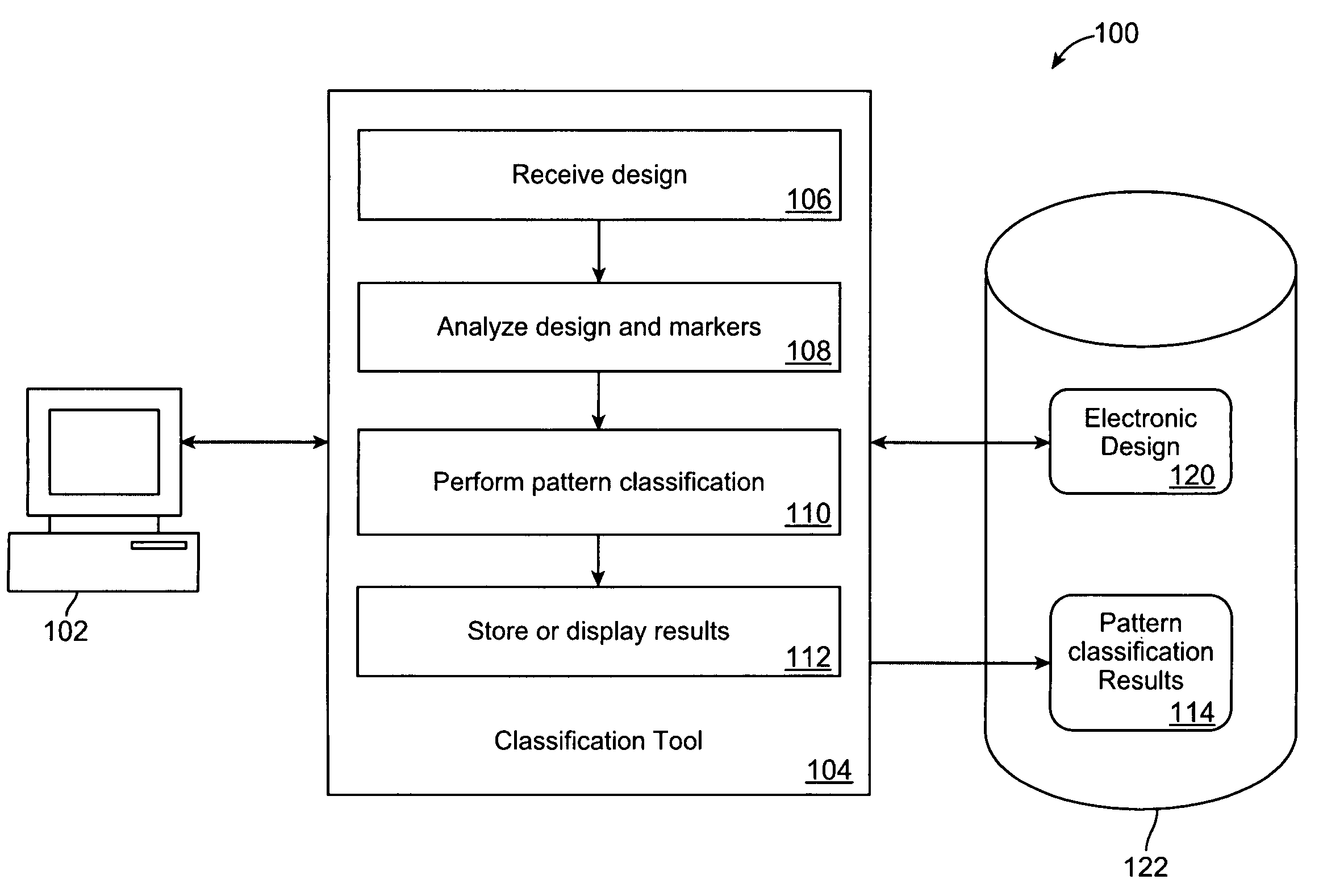
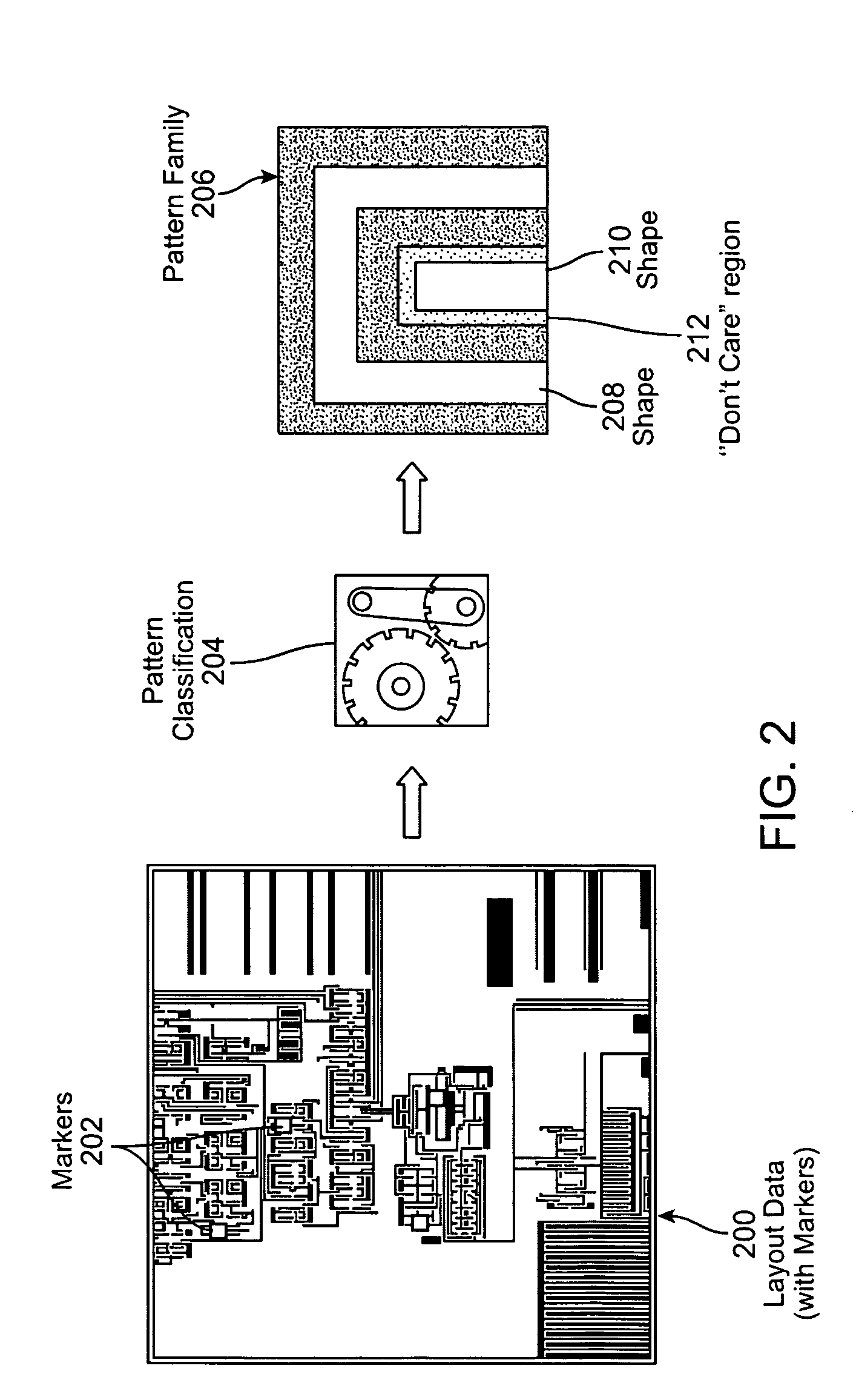
[0022]The present approach is directed to a method, system, and computer readable medium for performing pattern classification for electronic designs. One advantage of this invention it that it can use fast pattern matching techniques to classify both patterns and markers based on geometric similarity. In this way, the large number of markers and hotspots that typically are identified within an electronic design can be subsumed and compressed into a much smaller set of pattern families. This significantly reduced the number of patterns that must be individually analyzed, which considerably reduces the quantity of system resources and time needed to analyze and verify a circuit design.

[0023]The advantage of using geometric similarity is that there is often a large amount of geometric redundancy. This type of similarity can result in compression of information so there is less for a human to review. Further, geometric similarity is something that is intuitive to a human.

[0024]This app...


PUM


Abstract

Disclosed is an approach for performing pattern classification for electronic designs. One advantage of this approach is that it can use fast pattern matching techniques to classify both patterns and markers based on geometric similarity. In this way, the large number of markers and hotspots that typically are identified within an electronic design can be subsumed and compressed into a much smaller set of pattern families. This significantly reduced the number of patterns that must be individually analyzed, which considerably reduces the quantity of system resources and time needed to analyze and verify a circuit design.

Description

BACKGROUND AND SUMMARY[0001]The invention is directed to a more efficient approach for performing pattern classification with respect to patterns in integrated circuit designs.[0002]A semiconductor integrated circuit (IC) has a large number of electronic components, such as transistors, logic gates, diodes, wires, etc., that are fabricated by forming layers of different materials and of different geometric shapes on various regions of a silicon wafer. The various components of an integrated circuit are initially defined by their functional operations and relevant inputs and outputs. From the HDL or other high level description, the actual logic cell implementation is typically determined by logic synthesis, which converts the functional description of the circuit into a specific circuit implementation.[0003]An integrated circuit designer may use a set of EDA application programs to create a physical integrated circuit design layout from a logical circuit design. The EDA application ...

Claims


Application Information

Patent Timeline
Patent Type & Authority Patents(United States)
IPC IPC(8): G06F17/50
CPCG06F17/5081G06F2217/12G06F30/398G06F2119/18Y02P90/02
Inventor LAI, YA-CHIEHGENNARI, FRANK E.MOSKEWICZ, MATTHEW WLEI, JUNJIANGLAI, WEINONG
Owner CADENCE DESIGN SYST INC
Why Eureka
Try Eureka