Chiplet display with optical control

a chiplet display and optical control technology, applied in the field of display devices, can solve the problems of limiting the timing flexibility of the display, affecting the display performance, and affecting the display quality, so as to reduce the complexity of the display device, reduce the size and cost of the chiplet, and reduce the thickness of the display

Active Publication Date: 2011-12-20
GLOBAL OLED TECH
View PDF13 Cites 6 Cited by
  • Summary
  • Abstract
  • Description
  • Claims
  • Application Information

AI Technical Summary

Benefits of technology

[0017]An advantage of the present invention is that the chiplets are reduced in size and cost compared to the prior art. This can provide reduced display thickness compared to the prior art. Use of the selection circuit responsive to the pixel information is a more efficient design that reduces complexity of the display device. Furthermore, a display device of the present invention is more tolerant of wiring and interconnection faults than the prior art, as there can be no signal wires to fail. A further advantage is that the cost of driver circuitry and display manufacturing can be reduced compared to the prior art, as the number of electrical drivers to be bonded to the panel is reduced.
[0018]The present invention provides an effective way of optically distributing pixel information to chiplets on a flat panel display to control subpixels attached to those chiplets. Optical distribution removes delays experienced by electrical communications methods, including transmission-line and RLC delays. Transmitting light through the display backplane removes the need for a separate waveguide, and does not objectionably increase the volume occupied by the display. Forming photosensors on the chiplets permits the use of high-density lithography to form effective receiver circuits on the chiplets. The present invention does not increase manufacturing cost of the substrate as do prior art methods of substrate light-piping. The present invention provides robust communications with chiplets, which can be interrupted only by breaking the substrate.

Problems solved by technology

However, these configurations limit the timing flexibility of the display.
Furthermore, in active-matrix displays, each subpixel includes one or more thin-film transistors (TFTs), and such transistors have undesirable nonuniformity (e.g. low-temperature polysilicon, LTPS, TFTs) or aging (e.g. amorphous silicon, a-Si, TFTs).
However, in high-resolution or high-frame-rate displays, this technique is limited by the electrical properties of the row and column electrodes used to transmit pixel information, information controlling the subpixels, to the chiplets.
These electrodes have crosstalk and resistive, inductive and capacitive delays that are very difficult to overcome.
These schemes are not, therefore, suitable for flat-panel displays, which have significant constraints on space and particularly on thickness.
However, the poled electro-optical structures are complex and require expensive manufacturing processes.
Furthermore, this scheme is directed to a light output for pixels, a very different problem than control-signal distribution for chiplets.
However, in high-resolution displays, this scheme requires precise positioning of a large number of fibers, e.g. one per row.
Positioning errors can cause visible non-uniformity and reduce yields.

Method used


Image

  • Chiplet display with optical control
  • Chiplet display with optical control
  • Chiplet display with optical control

Examples


Embodiment Construction

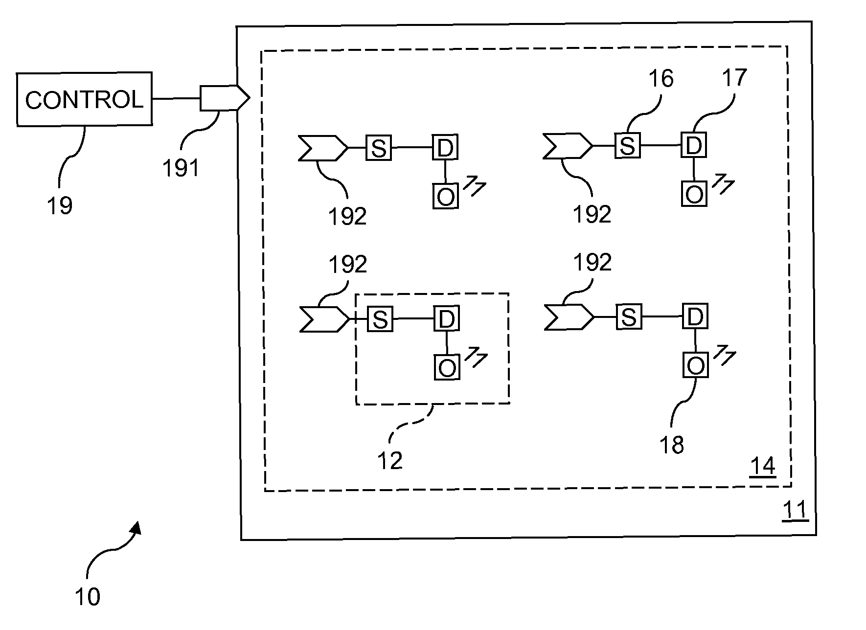
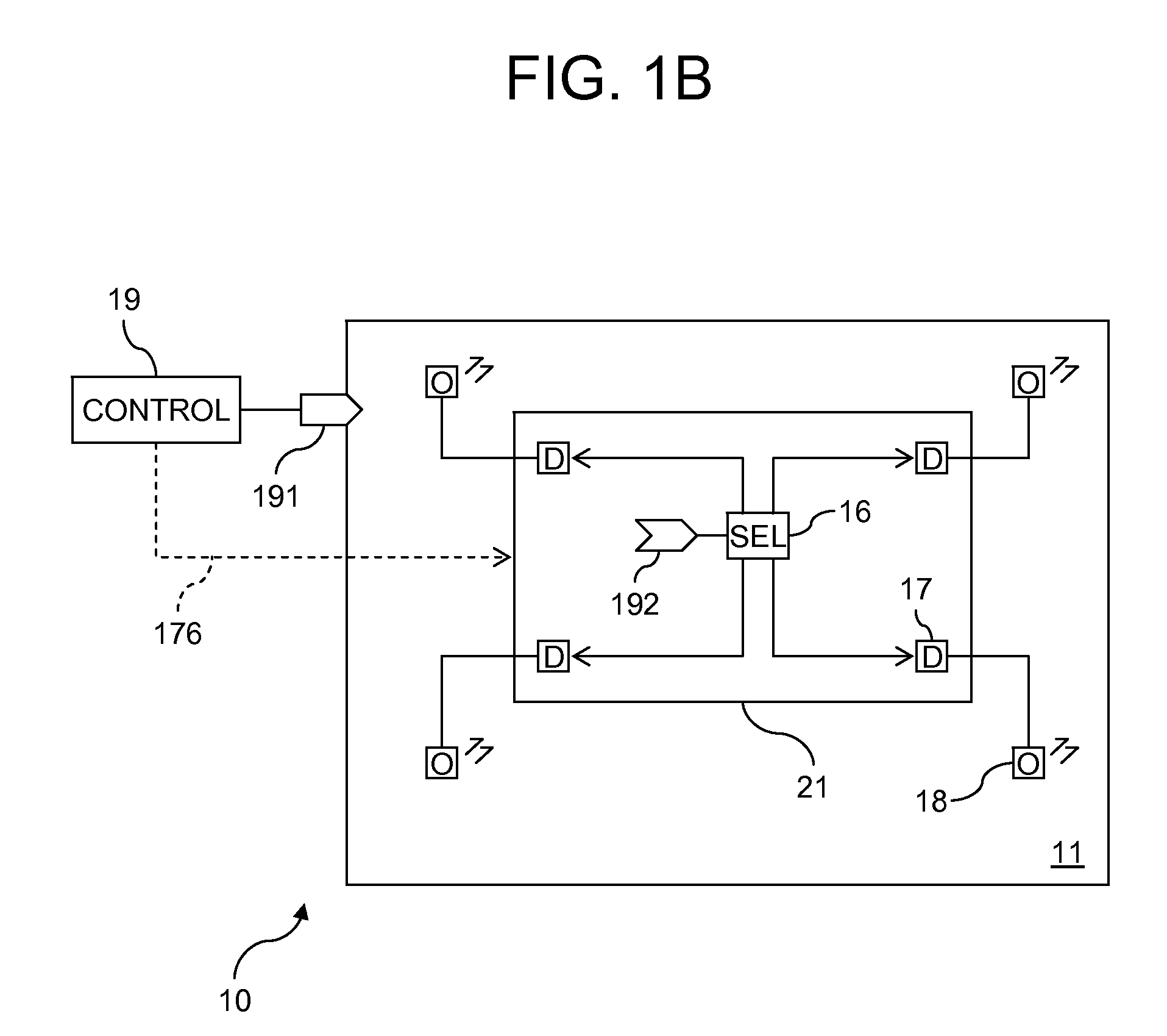
[0032]Referring to FIG. 1A, a display device 10 according to an embodiment of the present invention includes a display substrate 11 on which are formed a plurality of subpixels 12. Each subpixel 12 has a selection circuit 16 and a drive circuit 17. Each subpixel 12 also includes a display optical element 18, e.g. an electroluminescent (EL) emitter (light-emitting element). Each display optical element 18 is located in or over display area 14, and is responsive to the drive circuit for providing light. Connections within a subpixel 12 can be made electrically, optically, or by other ways known in the art. A controller 19 provides pixel information to each selection circuit 16 to determine how much light is provided by each subpixel 12.

[0033]The display substrate 11 defines an optical waveguide for transporting light carrying the pixel information. In this application, “light”, when referring to pixel information, includes all electromagnetic radiation (commonly called “radio waves”),...


PUM


Abstract

A display device having a display substrate defining an optical waveguide for transporting light carrying pixel information; a chiplet disposed over the display substrate, having a chiplet substrate separate from the display substrate, a photosensor responsive to light from the optical waveguide at the selected control wavelength for providing the pixel information, a selection circuit responsive to the pixel information for providing a control signal, and a drive circuit responsive to the control signal, wherein the chiplet is adapted to receive the transported light; an optical transmitter for transmitting the pixel information from the controller as light at the selected control wavelength into the optical waveguide, and a display optical element located in or over the display area responsive to the drive circuit for providing light.

Description

CROSS REFERENCE TO RELATED APPLICATION[0001]Reference is made to commonly-assigned, co-pending U.S. patent application Ser. No. 12 / 480,804 filed Jun. 9, 2009, entitled “Display Device with Parallel Data Distribution” to Cok et al, the disclosure of which is incorporated herein.FIELD OF THE INVENTION[0002]The present invention relates to display devices having a substrate with distributed, independent chiplets employing parallel control for a pixel array.BACKGROUND OF THE INVENTION[0003]Flat-panel display devices are widely used in conjunction with computing devices, in portable devices, and for entertainment devices such as televisions. Such displays typically employ a plurality of pixels distributed over a substrate to display images. The substrate is typically a continuous sheet of glass, but can be plastic or other materials, and can be divided into multiple adjacent tiles. Each pixel incorporates several, differently colored light-emitting elements commonly referred to as sub-pi...

Claims


Application Information

Patent Timeline
Patent Type & Authority Patents(United States)
IPC IPC(8): G06F3/038
CPCG09G3/2085G09G3/32G09G2370/18G09G2370/08G09G2360/141G09G3/30
Inventor WHITE, CHRISTOPHER J.HAMER, JOHN W.
Owner GLOBAL OLED TECH
Why Eureka
Try Eureka