Liquid crystal display panel and method for repairing signal line thereof

a technology of liquid crystal display panel and signal line, which is applied in the manufacture of electrode systems, electric discharge tubes/lamps, instruments, etc., can solve the problem of difficult disposal of repair lines b>16/b>, and achieve the effect of increasing the available periphery area of the substra

Active Publication Date: 2011-12-27
CHUNGHWA PICTURE TUBES LTD
View PDF2 Cites 19 Cited by
  • Summary
  • Abstract
  • Description
  • Claims
  • Application Information

AI Technical Summary

Benefits of technology

[0005]Accordingly, an objective of the present invention is to provide a display panel which the periphery area being occupied can be reduced, thereby overcoming the problems of the above-mentioned prior art.
[0006]Another objective of the present invention is to provide a method for repairing signal lines of the display panel. The signal lines can be repaired by the structure of the display panel without disposing a repair line.
[0020]In accordance with the display panel and the method for repairing the signal lines thereof, the problem that the repair line needs to be disposed on the periphery area of the substrate has been solved whereby a circuit route of simplified lighting replacing the repair line, thereby increases the available periphery area of the substrate.

Problems solved by technology

Therefore, the repair line 16 is difficult to be disposed.

Method used


Image

  • Liquid crystal display panel and method for repairing signal line thereof
  • Liquid crystal display panel and method for repairing signal line thereof
  • Liquid crystal display panel and method for repairing signal line thereof

Examples


first embodiment

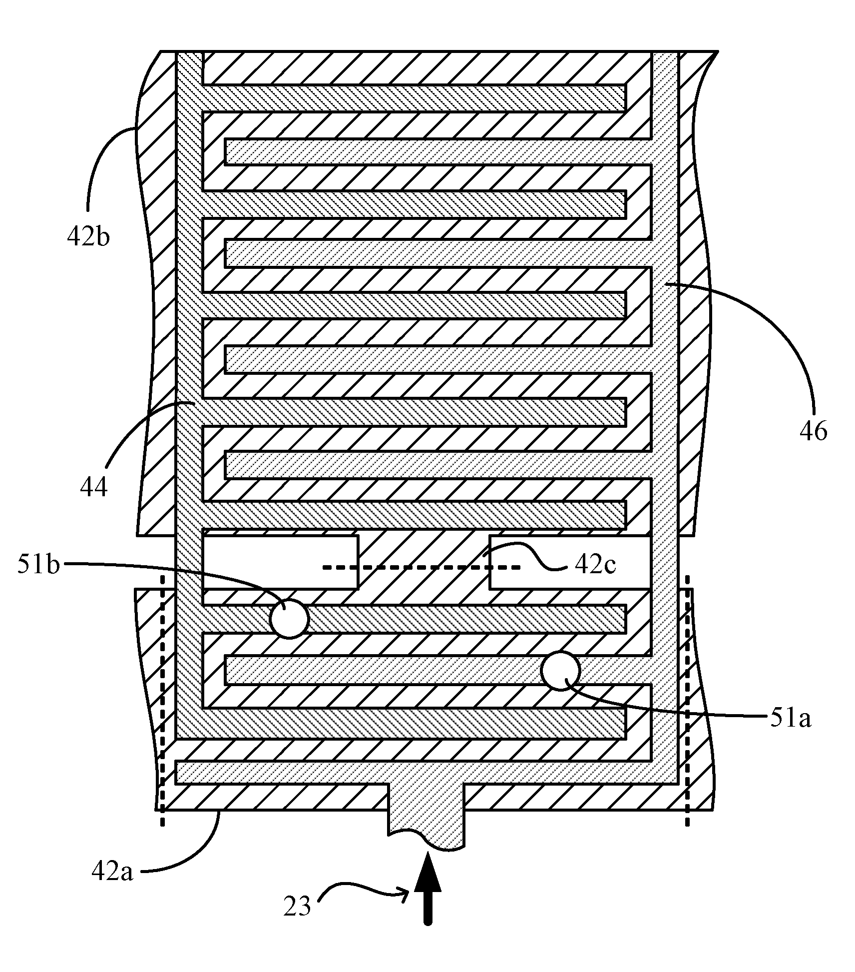
[0036]FIG. 5 is a top view illustrating a layout design of the switches in the present invention, which is utilized to explain the detailed structures of the switches 40. Referring to FIG. 5, the gate pattern 42 (designated as 42a, 42b and 42c) is disposed on the substrate 10, and the gate pattern 42 has a first region 42a and a second region 42b wherein the first region 42a and the second region 42b are connected by a connecting portion 42c. The manner for connecting the gate pattern 42a of any two adjacent switches 40 is that the first regions 42a are electrically coupled with each other and the second regions 42b thereof are electrically coupled with each other. It should be noted that the source line 44 and the drain line 46 expose the connecting portion 42c of the gate pattern 42.

[0037]The source line 44 is disposed on the gate pattern 42, and the insulation layer (not shown) is disposed between the source line 44 and the gate pattern 42 thereby serving as an insulator between ...

second embodiment

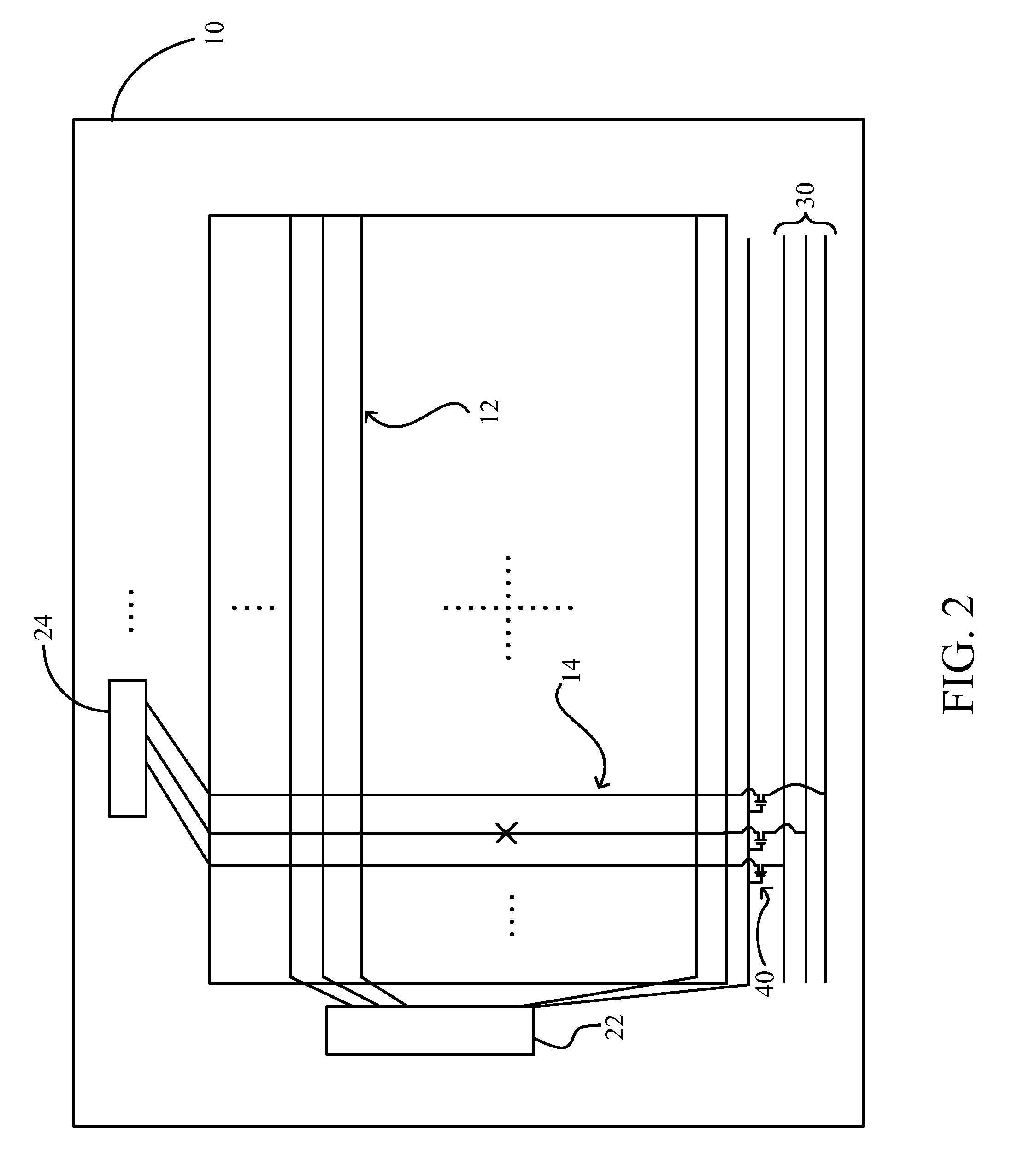
[0048]The display panel of thee present invention further includes a plurality of auxiliary repair lines 62. Both ends of each of the auxiliary repair lines 62 overlap one of a plurality of connections 39 between the switches 41 and the shorting bar group 30. An insulation layer (not shown) is disposed between the auxiliary repair lines 62 and the connections 39.

[0049]The source lines 45 of the switches 41, the drain lines 47 and the signal lines 14 are made of same metal material; for example, they are formed in the same manufacturing process in array process of the LCD panel. Similarly, the shorting bar group 30, the auxiliary repair lines 62 and the gate patterns 43 of the switches 41 are made of same metal material; for example, they are formed in the same manufacturing process in array process of the LCD panel. Therefore, it is not required to increase additional manufacturing processes.

[0050]The method for repairing the signal lines of the display panel in the second preferred...


PUM


Abstract

A display panel and a method for repairing signal lines thereof are disclosed. The display panel includes at least one shorting bar, switches, and auxiliary repair lines. The switches are electrically coupled respectively to signal lines and the at least one shorting bar. Both ends of each of the auxiliary repair lines overlap one of connections between the switches and the at least one shorting bar. When a signal line is damaged, the method for repairing includes: breaking off each of the connections between each of the switches and the at least one shorting bar by cutting; and welding both ends of one of the auxiliary repair lines which correspond to the damaged signal line with both sides of one of the connections which correspond to the damaged signal line.

Description

TECHNICAL FIELD OF THE INVENTION[0001]The present invention relates to a display panel, and especially to a liquid crystal display (LCD) panel and a method for repairing signal lines thereof.BACKGROUND OF THE INVENTION[0002]FIG. 1 is a top view schematically illustrating a repairing of a signal line in a conventional liquid crystal display (LCD) panel. Referring to FIG. 1, the LCD panel includes a substrate 10, which comprises a plurality of scan lines 12 and a plurality of signal lines 14, and the scan lines 12 are parallel to each other and cross the signal lines 14. A plurality of pixel regions and a thin film transistor (TFT) array are defined between the scan lines 12 and the signal lines 14 (not shown). In addition, the substrate 10 comprises a scan line driver chip 22 and a plurality of signal line driver chips 24, in which only a signal line driver chip 24 is depicted for clarity. The scan line driver chip 22 is utilized to drive the scan lines 12 in sequence, and the signal...

Claims


Application Information

Patent Timeline
Patent Type & Authority Patents(United States)
IPC IPC(8): H01J9/50G09G3/30
CPCG02F1/136259G09G3/2092G02F1/136204G09G3/3648G09G2330/08G02F2001/136263G02F1/136263
Inventor HUANG, JUN-YAOTENG, YIN-HSIANGHUNG, REN-TSAICHEN, HAN-CHANGHAN, CHIA-JUNG
Owner CHUNGHWA PICTURE TUBES LTD
Why Eureka
Try Eureka