Semiconductor memory device

a memory device and semiconductor technology, applied in the direction of semiconductor/solid-state device manufacturing, semiconductor devices, electrical apparatus, etc., can solve the problems of unsuitable structure for large capacity and concern about short circui

Active Publication Date: 2012-01-03
KIOXIA CORP
View PDF5 Cites 40 Cited by
  • Summary
  • Abstract
  • Description
  • Claims
  • Application Information

AI Technical Summary

Problems solved by technology

This structure is unsuitable for large capacity because it requires many manufacturing steps per layer.
Depending on the slit pattern layout, there is concern about the problem of short circuit between the word line electrode layers of adjacent blocks or regions across the slit through the residual electrode layers beside the slit.

Method used


Image

  • Semiconductor memory device
  • Semiconductor memory device
  • Semiconductor memory device

Examples


Embodiment Construction

[0023]An embodiment of the invention will now be described with reference to the drawings.

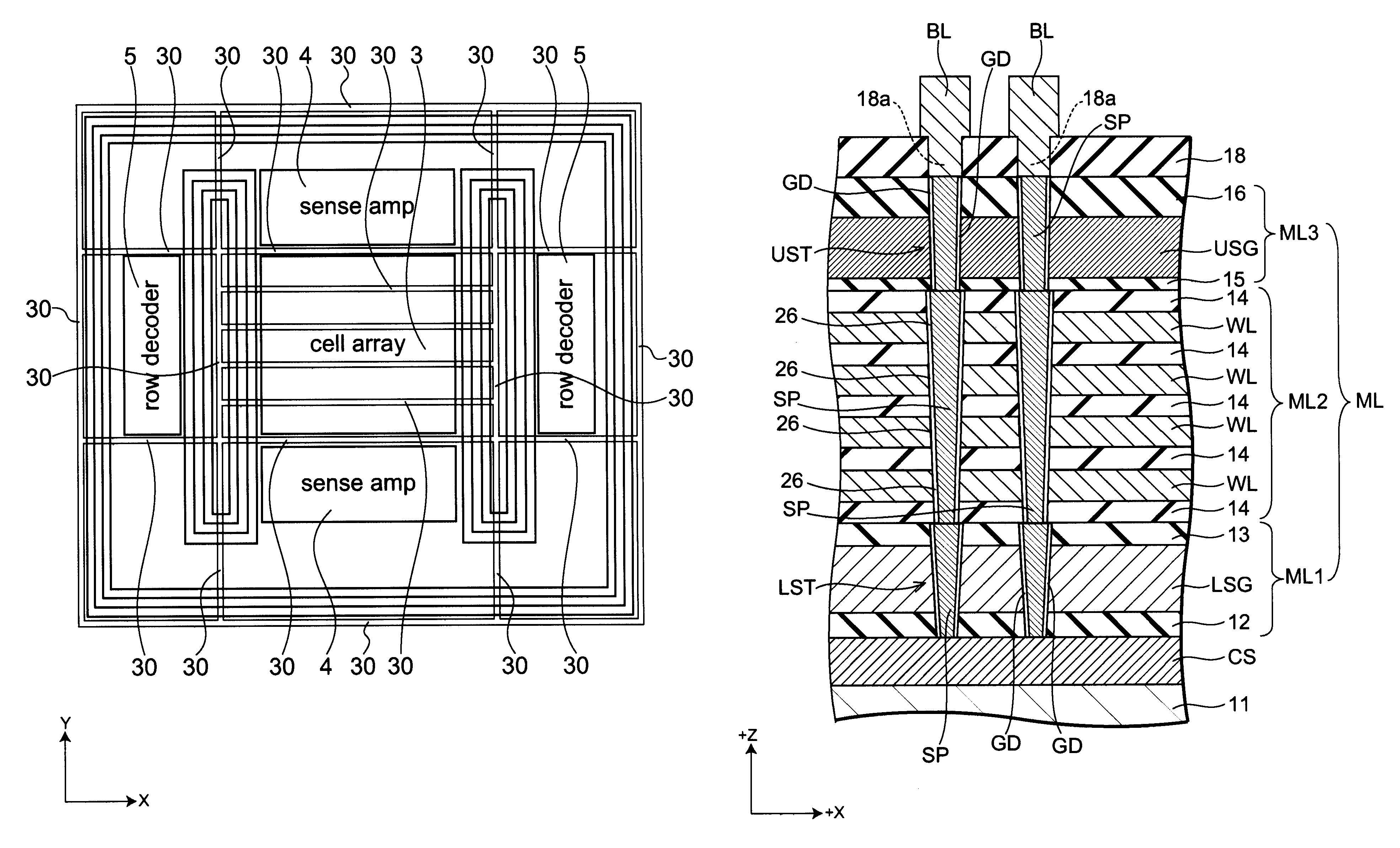
[0024]FIG. 1 is a schematic view illustrating the planar layout of major components in a semiconductor memory device according to the embodiment of the invention.

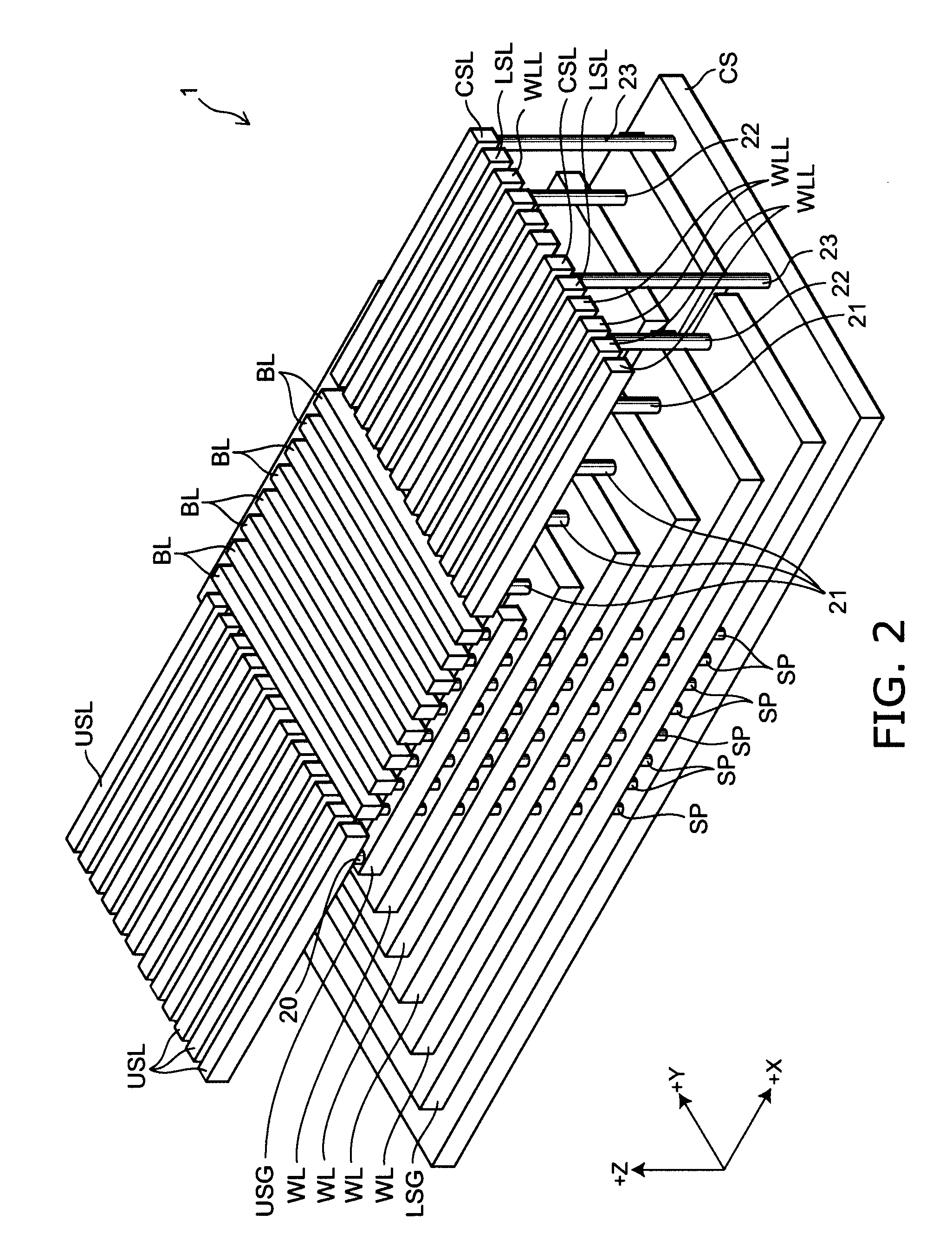
[0025]FIG. 1 shows one chip region, which is broadly divided into a memory cell array region and a peripheral circuit region. The memory cell array region is formed at the center of the chip and includes memory cells 3. The peripheral circuit region is formed around the memory cell array region and includes a sense amplifier 4, row decoder 5, and other circuits.

[0026]A stacked body with a plurality of conductive layers and a plurality of dielectric layers alternately stacked, described later, is provided throughout the chip including the memory cell array region and the peripheral circuit region. The stacked body is divided by slits 30 into a plurality of blocks. An interlayer dielectric film is buried in the slit 30 as described later...


PUM


Abstract

A semiconductor memory device includes: a semiconductor substrate; a stacked body with a plurality of conductive layers and a plurality of dielectric layers alternately stacked, the stacked body being provided on the semiconductor substrate; a semiconductor layer provided inside a hole formed through the stacked body, the semiconductor layer extending in stacking direction of the conductive layers and the dielectric layers; and a charge storage layer provided between the conductive layers and the semiconductor layer. The stacked body in a memory cell array region including a plurality of memory strings is divided into a plurality of blocks by slits with an interlayer dielectric film buried therein, the memory string including as many memory cells series-connected in the stacking direction as the conductive layers, the memory cell including the conductive layer, the semiconductor layer, and the charge storage layer provided between the conductive layer and the semiconductor layer, and each of the block is surrounded by the slits formed in a closed pattern.

Description

CROSS-REFERENCE TO RELATED APPLICATIONS[0001]This application is based upon and claims the benefit of priority from the prior Japanese Patent Application No. 2008-282817, filed on Nov. 4, 2008; the entire contents of which are incorporated herein by reference.BACKGROUND OF THE INVENTION[0002]1. Field of the Invention[0003]This invention relates to a semiconductor memory device having a three-dimensional memory cell array structure in which electrode layers are stacked to form memory cells densely arranged in the electrode stacking direction.[0004]2. Background Art[0005]Conventional stacked memory technology is based on the structure of layers stacked by repeating for each layer the process of forming normal, planar memory cells on a silicon substrate. This structure is unsuitable for large capacity because it requires many manufacturing steps per layer. In this context, a technique for increasing the capacity with high manufacturing efficiency is proposed (e.g., JP-A-2007-266143(Kok...

Claims


Application Information

Patent Timeline
Patent Type & Authority Patents(United States)
IPC IPC(8): H01L29/792H01L29/94H01L31/062H01L31/113H01L29/76
CPCH01L27/11582H01L27/11578H10B43/20H10B43/27H01L27/0688
Inventor TANAKA, HIROYASUKIDOH, MASARUKATSUMATA, RYOTAKITO, MASARUKOMORI, YOSUKEISHIDUKI, MEGUMIAOCHI, HIDEAKIFUKUZUMI, YOSHIAKI
Owner KIOXIA CORP
Why Eureka
Try Eureka