Solid state thermoelectric power converter

a thermoelectric power converter and solid-state technology, applied in the direction of thermoelectric devices with peltier/seeback effect, basic electric elements, electric devices, etc., to achieve the effect of increasing the surface area available for cooling and improving the efficiency of power conversion

Inactive Publication Date: 2012-01-24
TE ENERGY LLC A FLORIDA LLC
View PDF2 Cites 20 Cited by
  • Summary
  • Abstract
  • Description
  • Claims
  • Application Information

AI Technical Summary

Benefits of technology

[0024]It is a further purpose of this invention to provide a means to energize the control board and thereby replace the need for a battery in the device.
[0025]It is a further purpose of this invention to improve the efficiency of power conversion by splitting the ends of cold fins and thereby increasing the surface area available for cooling.

Problems solved by technology

Thermoelectric generator devices have been used for many years for specific applications where the simplicity of design warrants their use despite low energy conversion efficiency.

Method used


Image

  • Solid state thermoelectric power converter
  • Solid state thermoelectric power converter
  • Solid state thermoelectric power converter

Examples


example 1

Reduced Barriers N-Type Semiconductor Composition

[0166]

Preferred ElementRangeAmountSelenium 5% - 12%10%Bismuth40% - 60%45%Telluriumremainder to 100%45%

[0167]This n-type selenium-bismuth-telluride-based semiconductor composition represents a formula [Bi2Te3]0.35[Bi2Se3]0.65 approximating a ratio of one part dibismuth tritelluride and two parts dibismuthtriselenide. This product appears to be crystalline.

example 2

Reduced Barriers P-Type Semiconductor Composition

[0168]Element Range Preferred Amount

[0169]

Antimony28% - 32%30%Bismuth 8% - 12%10%Telluriumremainder to 100%60%

[0170]This p-type antimony-bismuth-telluride-based semiconductor composition represents a formula [Bi2Te3]0.35[Sb2Te3]0.65 or about one part dibismuthtritelluride and 2 parts diantimonytritelluride. Diantimonytritelluride structural form is a glass. The structure of dibismuth-tetraantimony-nonatelluride as produced by the method described herein appears to be crystalline.

[0171]Copper and some other elements greatly degrade performance of these semiconductors; therefore high purity elements are needed. Each chemical element should be at least 99.9% pure and preferably 99.999% pure.

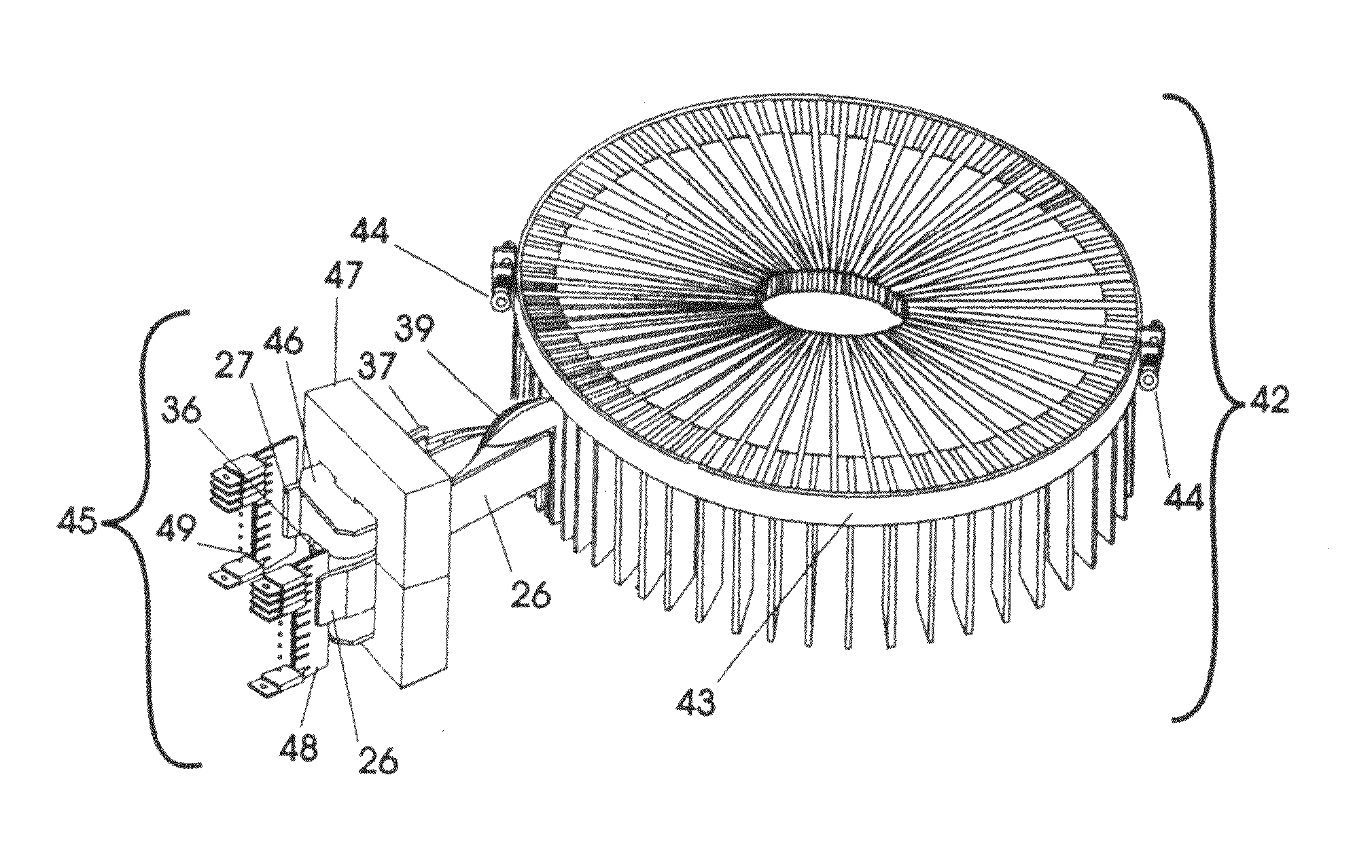
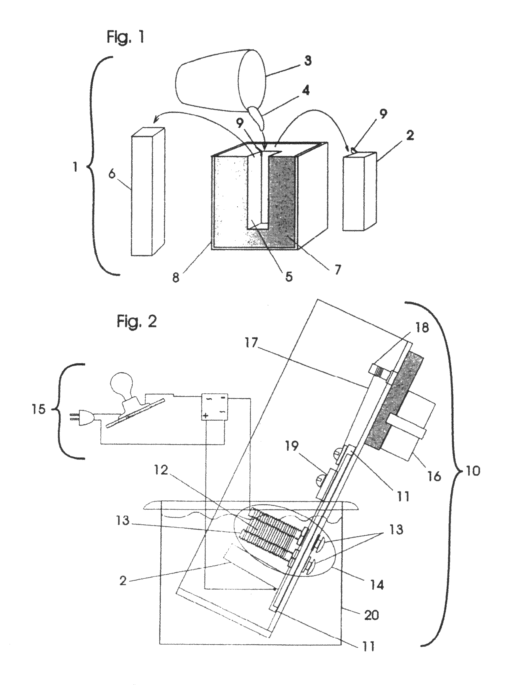
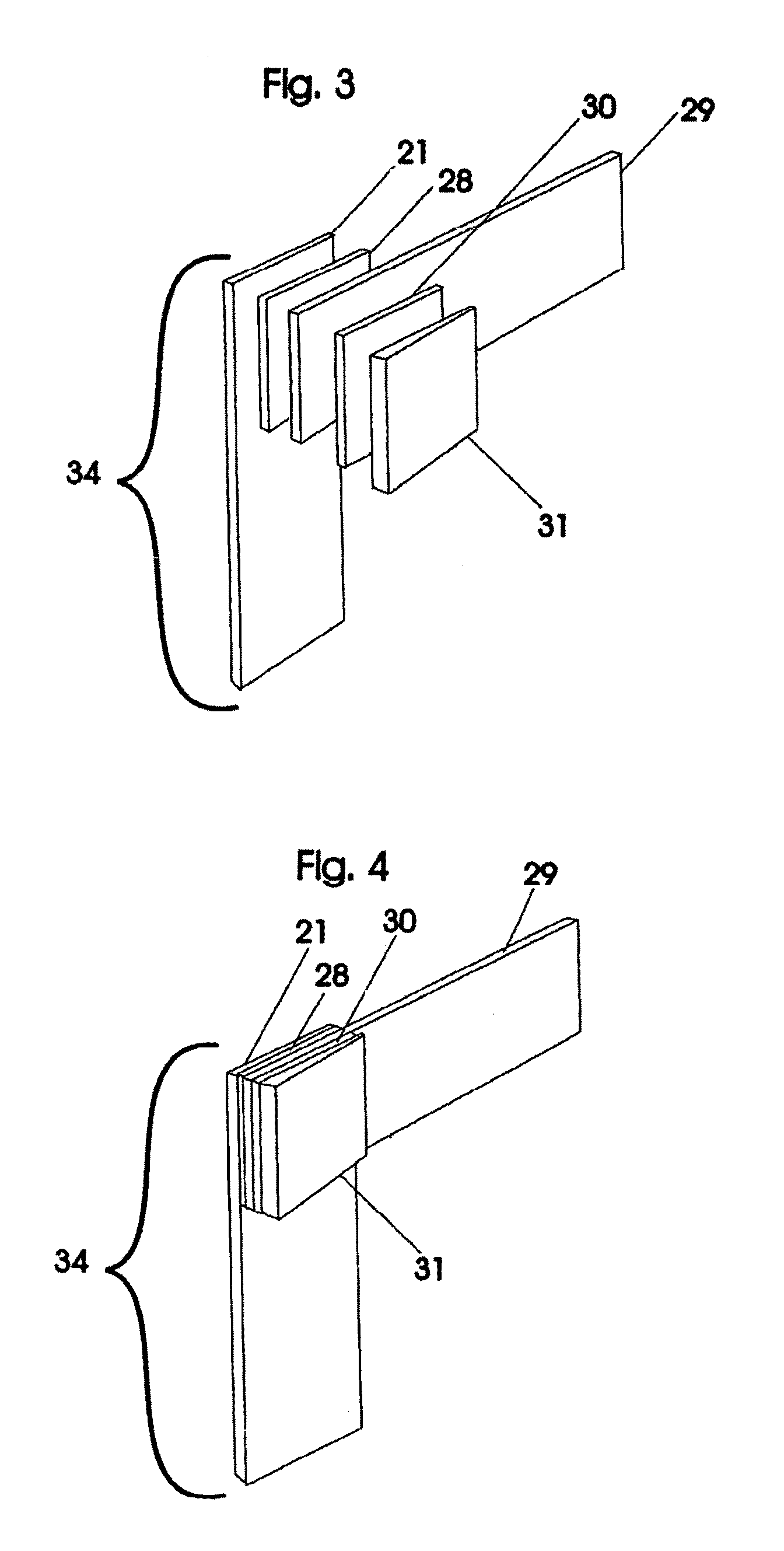
[0172]Semiconductors are protected from infiltration of copper atoms and components of solder by first coating the wafer edges with a non-conductive high temperature-melting ink, brand named “mark-tex” high temp 44 manufactured by DYKEM, preferably co...


PUM


Abstract

High efficiency conversion of heat energy to electrical energy is achieved using a ring of metallic components and anodically sliced, reduced barriers, high purity n-type and p-type semiconductor wafers. Energy produced by heating one set of fins and cooling another set is extracted from a ring of bismuth telluride based n-type wafers and antimony telluride based p-type wafers using make-before-break control of MOSfet switch banks. Standard AC frequencies and DC output result from rectification of make-before-break high frequency switched very high currents in the ring and a DC to AC converter. Solar energy stored in porcelain fragments extends the time that solar energy can be used as the heat source for the thermoelectric generator device.

Description

RELATED APPLICATIONS[0001]This application is a continuation-in-part of U.S. patent application Ser. No. 10 / 154,757, filed May 23, 2002, now abandoned entitled “Torus Semiconductor Thermoelectric Device” published Nov. 27, 2003.TECHNICAL FIELD[0002]This invention relates to a circular array of semiconductor and conductive elements that comprise a high efficiency thermoelectric generator device. Energy generated by a temperature differential between hot and cold fins of the thermoelectric generator device is more efficiently converted to electrical energy by a combination of both high efficiency semiconductor elements and a high frequency direct current to direct current switching component. When combined with an H-bridge the combination produces alternating current output of various standard voltages and frequencies. Improved cooling efficiency is obtained by increasing the surface area of the cold fins. This is accomplished by splitting and displacing the lower portion of the cold ...

Claims


Application Information

Patent Timeline
Patent Type & Authority Patents(United States)
IPC IPC(8): H01L35/00H01L35/30
CPCH01L35/30H10N10/13
Inventor SCHROEDER, JON MURRAYHIRSCH, GERALD PHILIP
Owner TE ENERGY LLC A FLORIDA LLC
Why Eureka
Try Eureka