Proximity communication package for processor, cache and memory

a technology of cache and memory, applied in the direction of electrical apparatus construction details, instruments, semiconductor/solid-state device details, etc., can solve the problems of limiting the ability of processors to utilize advancements in computational power, and affecting the performance of the processor. achieve the effect of reducing the topology variation of the cache memory

Active Publication Date: 2012-01-24
ORACLE INT CORP
View PDF13 Cites 14 Cited by
  • Summary
  • Abstract
  • Description
  • Claims
  • Application Information

AI Technical Summary

Benefits of technology

[0020]In various example embodiments, the bridge has a thickness of less than 150 micrometers, and / or a compliance ranging between 20 and 30 micrometers to mitigate topology variations of the cache memory, processor and / or substrate(s) or components that physically support or locate them.

Problems solved by technology

Driving bandwidth off a processor chip to L3 cache with low latency presents challenges, especially as processor technology continues to scale to future generations.
The latency for this communication will continue to be impeded by the inability for electrical signaling to drive off chip without penalty.
For example today's 10 Gbps serial links drive off chip to cache at a cost of several nanoseconds or several hundreds of processor clock cycles This can limit the ability of processors to utilize advancement in computational power, clock frequency, transistor count, multi-coring and so forth.
Actual details can be more complex, including for example chip logic for driving and amplifying the signals, and the receiver circuit must tolerate far more variation than a conductive connection.
Technologies in 2004 were limited to a few hundred gigabytes per second.
Wafer scale integration has historically failed because the yield (e.g., known good die) drops to zero as the silicon area of a chip increases.
This can be very expensive or impossible with prior art methods that connect chips to multi-chip modules, and force replacement of the entire circuit module instead of just the defective part.
Although proximity communication as a means to signal between processor and memory could alleviate the issue or challenge of driving bandwidth off a processor chip to L3 cache with low latency, a problem is that proximity signaling near the processor cannot be packaged in a low cost solution using industry standard packaging platforms.
This is because proximity signaling needs tolerances much smaller than 10 microns to accomplish high fidelity signaling whereas manufacturing cannot achieve tolerance of better than a few mils or thousandths of an inch at low cost.
One of the issues with packaging proximity commutation is overcoming the flatness tolerances of first-level packages.
There are additional manufacturability issues associated with the “known good die” problem.
Solutions such as Multichip Modules (MCM) have only a limited impact in packaging technology today owing to the known good die problem and the inability to significantly test chips until parts are packaged into the full assembly.

Method used


Image

  • Proximity communication package for processor, cache and memory
  • Proximity communication package for processor, cache and memory
  • Proximity communication package for processor, cache and memory

Examples


Embodiment Construction

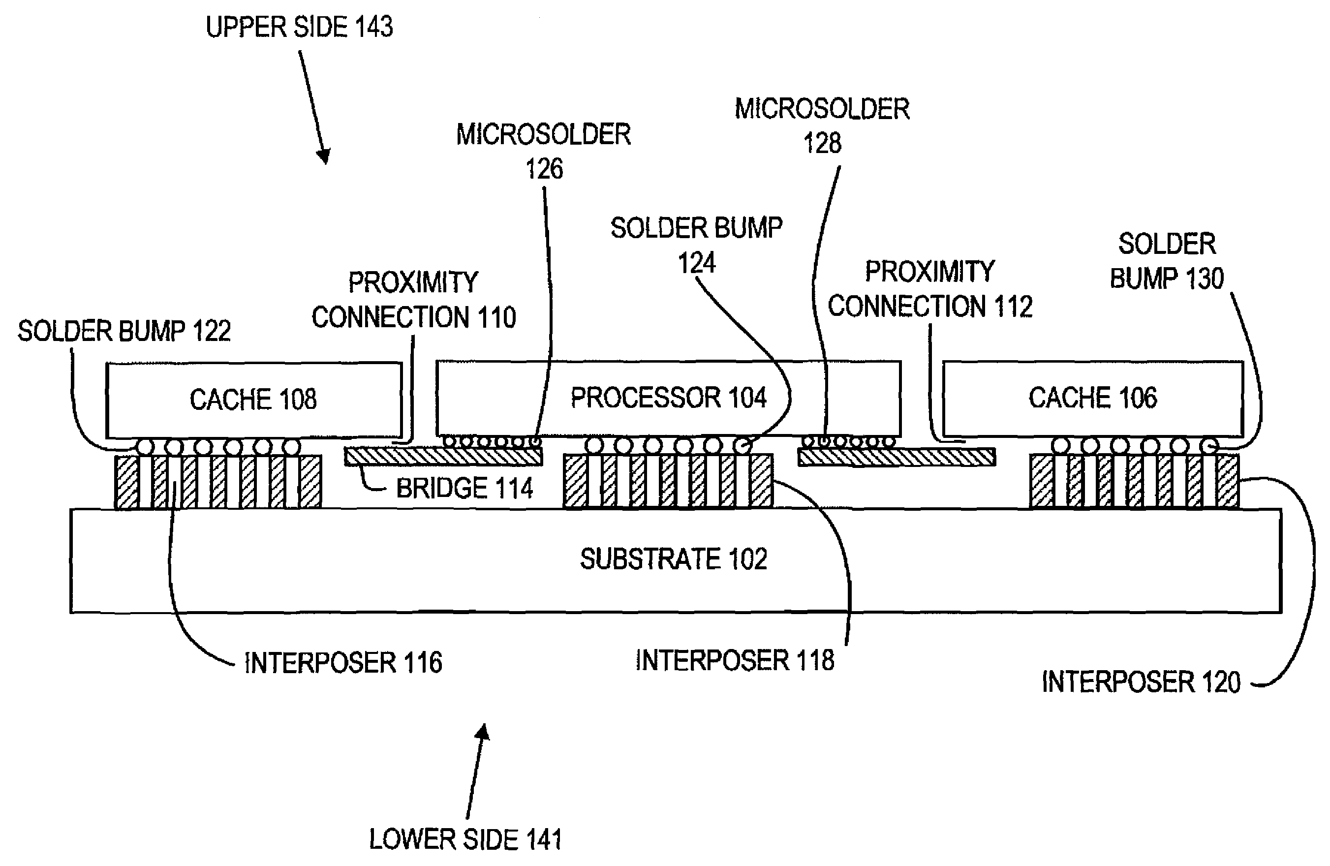
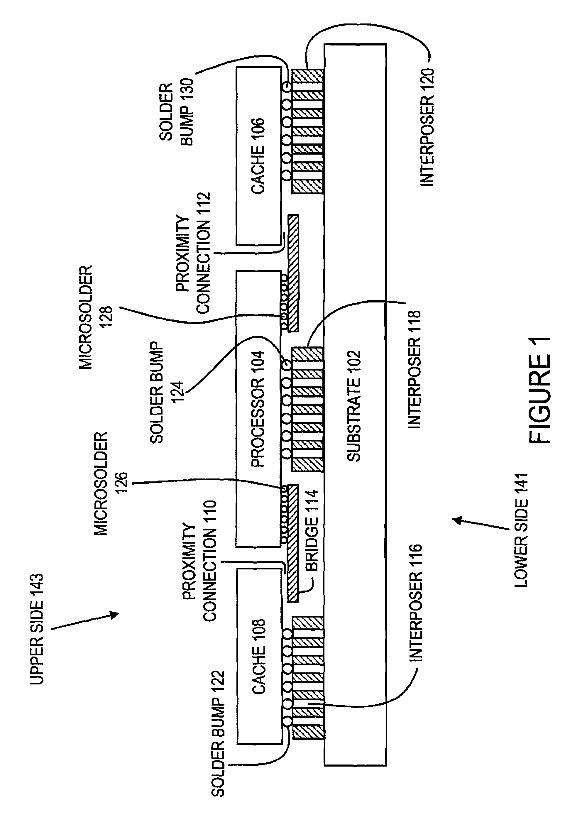
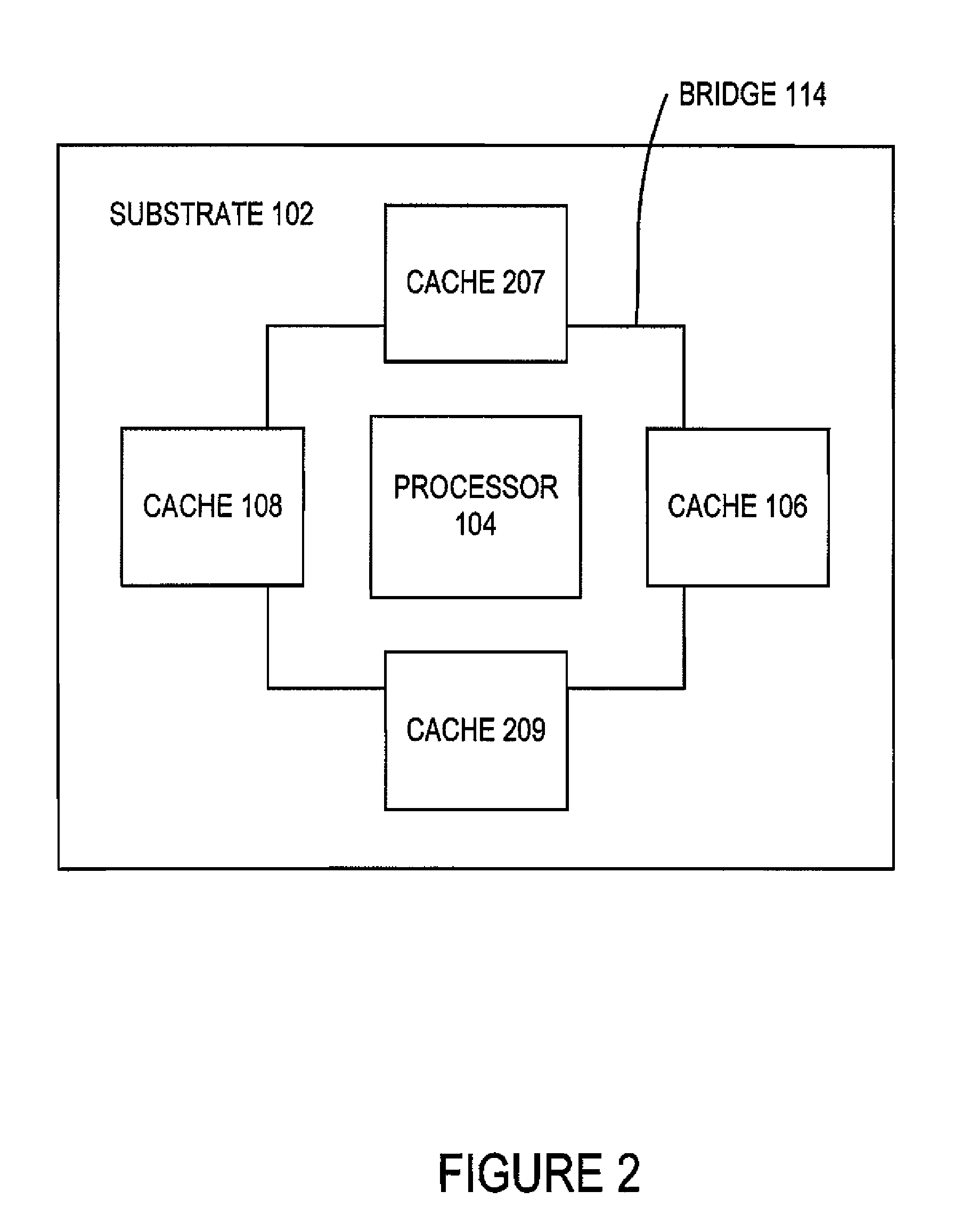
[0029]The present invention now will be described more fully hereinafter with reference to the accompanying drawings, which form a part hereof, and which show, by way of illustration, specific embodiments by which the invention may be practiced. This invention may, however, be embodied in many different forms and should not be construed as limited to the embodiments set forth herein; rather, these embodiments are provided so that this disclosure will be thorough and complete, and will fully convey the scope of the invention to those skilled in the art. Among other things, the present invention may be embodied as methods or devices. Accordingly, the present invention may take the form of an entirely hardware embodiment, or an embodiment combining software and hardware aspects. The following detailed description is, therefore, not to be taken in a limiting sense.

[0030]Throughout the specification and claims, the following terms take the meanings explicitly associated herein, unless th...


PUM


Abstract

A “sombrero” bridge transports signal communication between a processor and one or more cache memories. The bridge surrounds the processor's perimeter, and includes an aperture opposite the processor through which power and data can be provided to the processor from another device. The bridge exchanges signals with the cache memories via capacitively coupled proximity connections. The bridge communicates with the processor via conductive (e.g. wire) connections and optionally proximity connections. Spacing between opposing pads of the proximity connection(s) between the bridge and the cache memories can be provided by recesses in a surface of the cache memory, corresponding recesses in an opposing surface of the bridge, and a ball for each matching pair of corresponding cache memory and bridge recesses. The ball fits in and between the recesses of the matching pair. The recess depths and ball diameter(s) constrain a minimum distance between opposing pads of the proximity connection(s).

Description

GOVERNMENT LICENSE RIGHTS[0001]The United States Government has a paid-up license in this invention and the right in limited circumstances to require the patent owner to license others on reasonable terms as provided for by the terms of Agreement No. NBCH020055 awarded by the Defense Advanced Research Projects Administration (DARPA).FIELD OF THE INVENTION[0002]Embodiments of the invention are directed to packaging solutions to enable Proximity Communication of signals between a processor and cache memory.BACKGROUND[0003]Driving bandwidth off a processor chip to L3 cache with low latency presents challenges, especially as processor technology continues to scale to future generations. In a few years a processor will need serial data rates of many 10 Gbps over many channels of communication to cache. The latency for this communication will continue to be impeded by the inability for electrical signaling to drive off chip without penalty. For example today's 10 Gbps serial links drive o...

Claims


Application Information

Patent Timeline
Patent Type & Authority Patents(United States)
IPC IPC(8): H05K7/00
CPCH01L23/48H01L24/73H01L25/18H01L2924/00014H01L2924/10253H01L2225/06531H01L2224/45147H01L2924/01033H01L25/0652H01L2225/06513H01L2924/01013H01L2924/01029H01L2924/01032H01L2924/01049H01L2924/14H01L2924/19041H01L2924/01006H01L2924/01023H01L2924/00H01L2224/48H01L2924/15787H01L2224/1403H01L2224/16227H01L2224/16235H01L2224/1703
Inventor CUNNINGHAM, JOHN E.KRISHNAMOORTHY, ASHOK V.LANDIN, ANDERS
Owner ORACLE INT CORP
Why Eureka
Try Eureka