Semiconductor device

a technology of semiconductor devices and semiconductors, applied in semiconductor devices, digital storage, instruments, etc., can solve the problems of pushing up the manufacturing cost of semiconductor devices, and achieve the effect of suppressing an increase in the layout area of chips and high precision

Active Publication Date: 2012-01-24
LONGITUDE LICENSING LTD
View PDF5 Cites 0 Cited by
  • Summary
  • Abstract
  • Description
  • Claims
  • Application Information

AI Technical Summary

Benefits of technology

[0046]In the above, sensitive element requiring high-precision controls of threshold voltage is not disposed in the peripheral region suffering from uneven impurity density close to the boundary in the well but is distanced from the boundary and disposed in the center region having uniform impurity density inside the well, wherein the center region is designed to have the prescribed impurity density determined in advance. This prevents unwanted variations of the impurity density inside the well so as to control operational characteristic parameters of sensitive element at a high precision. In addition, non-sensitive elements allowing low-precision control of threshold voltage is disposed in peripheral region suffering from uneven impurity density; thus, it is possible to suppress an increase in the layout area of chips.

Problems solved by technology

This pushes up the manufacturing cost for manufacturing semiconductor devices having numerous sense amplifier circuits due to high memory capacities.

Method used


Image

  • Semiconductor device
  • Semiconductor device
  • Semiconductor device

Examples


Embodiment Construction

[0065]The present invention will now be described herein with reference to illustrative embodiments. Those skilled in the art will recognize that many alternative embodiments can be accomplished using the teachings of the present invention and that the invention is not limited to the embodiments illustrated for explanatory purposes.

[0066]The present invention is directed to a decrease in negative influences on the semiconductor device's performance due to dispersion of impurity density in a process for the manufacture of the semiconductor devices.

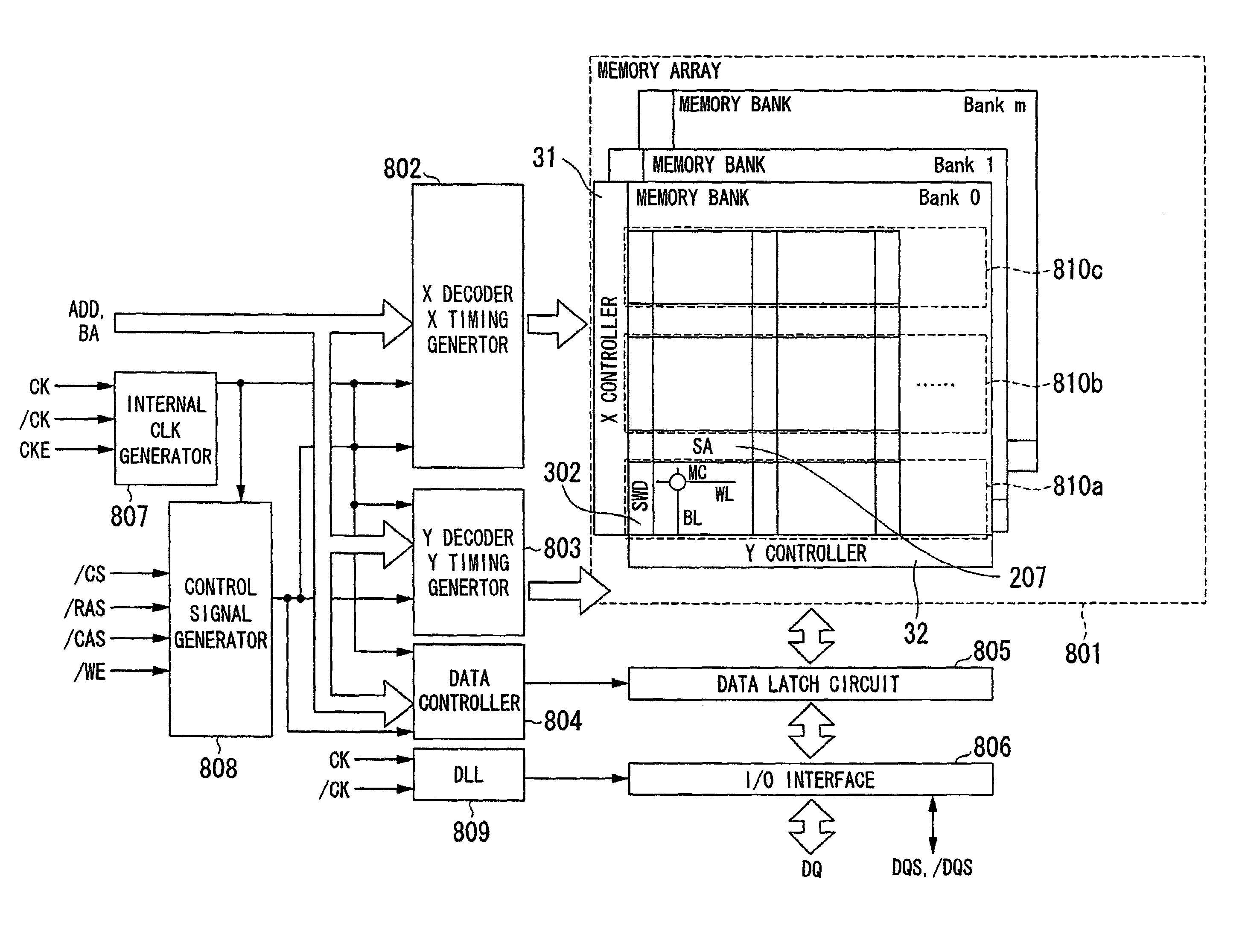
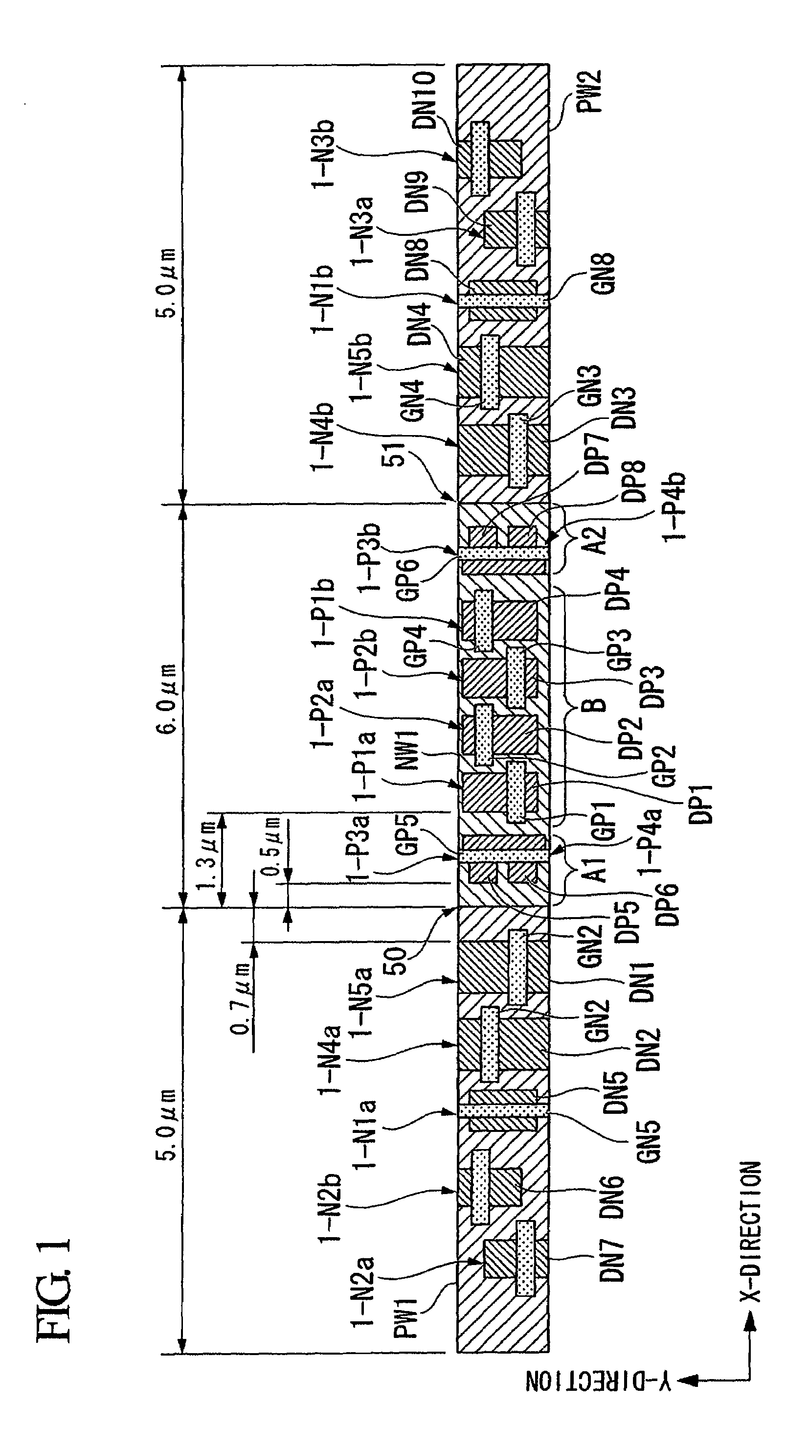
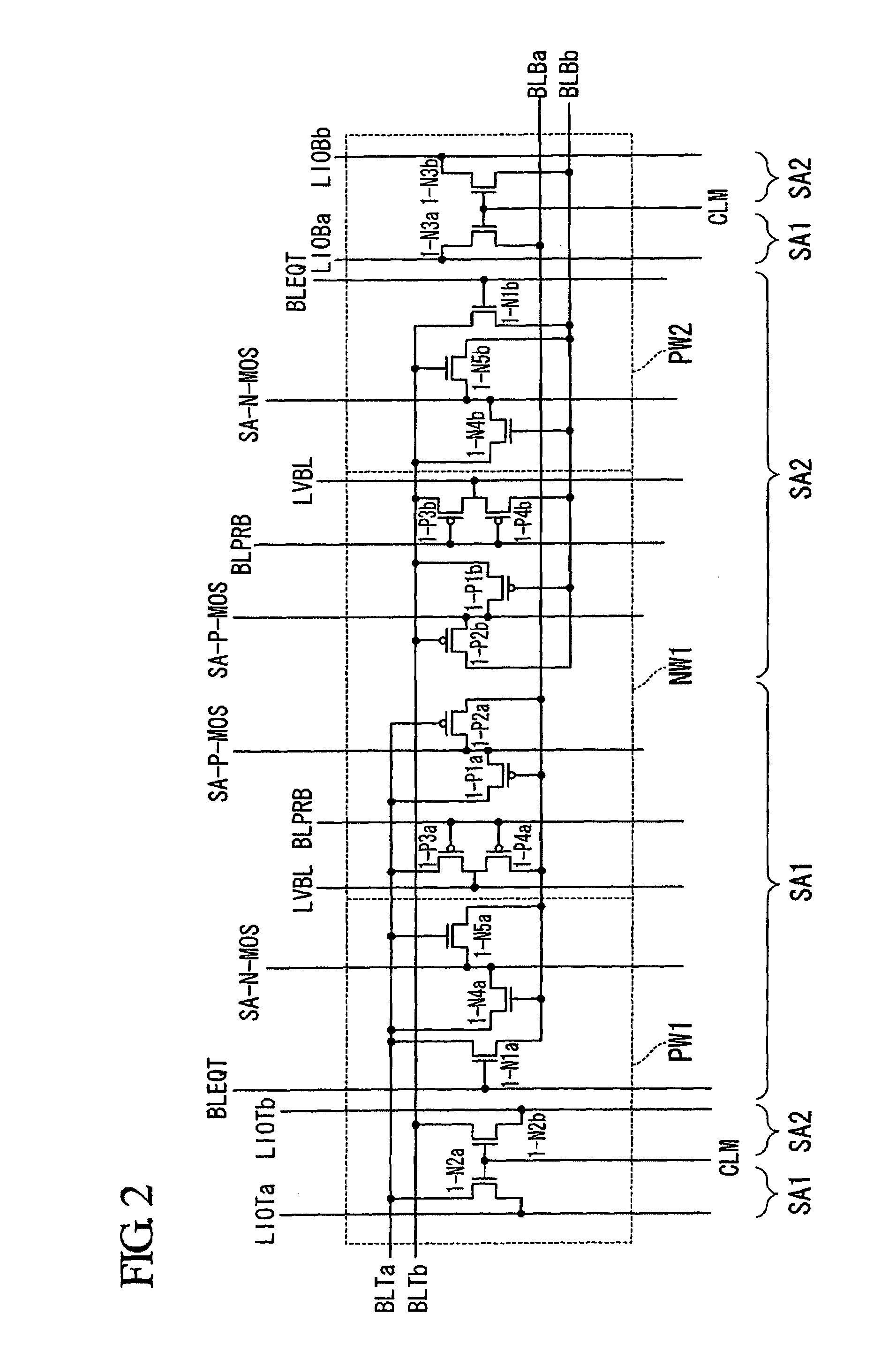
[0067]FIG. 1 is a plan view showing the layout of a sense amplifier circuit and its associated elements formed in wells of a sub-cell array of a dynamic random-access memory (DRAM) according to the present embodiment, wherein parts identical to those shown in FIG. 7 are designated by the same reference numerals; hence, the duplicate descriptions thereof are simplified or omitted as necessary.

[0068]The following description is given with res...


PUM


Abstract

A semiconductor device includes a plurality of memory cells and a sense amplifier circuit which further includes a plurality of elements such as MOS transistor formed in a well, wherein sensitive element, which are sensitive to dispersion of an impurity density in the well, is distanced from a boundary and are disposed in the center region of the well, while non-sensitive element is disposed in the peripheral region close to the boundary in the well. Since sensitive element requiring precise control of threshold voltage is disposed in the center region having uniform impurity density, and non-sensitive element allowing for less precise control of threshold voltage is disposed in the peripheral region suffering from uneven impurity density, it is possible to effectively use the overall area of the well and to thereby suppress an increase in the layout area of chips.

Description

BACKGROUND OF THE INVENTION[0001]1. Field of the Invention[0002]The present invention relates to semiconductor devices and in particular, a decrease in negative influences on the semiconductor device's performance due to dispersion of impurity density in a process for the manufacture of the semiconductor devices.[0003]The present application claims priority on Japanese Patent Application No. 2008-293349, the content of which is incorporated herein by reference.[0004]2. Description of Related Art[0005]Dynamic random-access memories (DRAM) are constituted of memory cells, each of which is configured of a single capacitor for accumulating data and a single switching transistor for reading and writing data with the capacitor.[0006]Progressing highly integrated structures of memories reduces the amount of charges accumulated in capacitors so as to reduce magnitudes of signals read from capacitors by switching transistors; hence, they require sense amplifiers to amplify signals having sma...

Claims


Application Information

Patent Timeline
Patent Type & Authority Patents(United States)
IPC IPC(8): G11C7/02
CPCH01L27/10897H01L27/088H01L27/10894H01L27/0207H01L21/26586H01L21/823412H10B12/50H10B12/09
Inventor MATSUMOTO, YASUHIROKOSHIKAWA, YASUJI
Owner LONGITUDE LICENSING LTD
Why Eureka
Try Eureka