Reflective mask blank for EUV lithography and reflective mask for EUV lithography

a technology of reflective masks and euv lithography, which is applied in the field of reflective masks for euv lithography, can solve the problems of accelerating microsizing of semiconductor devices and the resolution limit of conventional photolithography, and achieve excellent shape accuracy and dimensional accuracy

Inactive Publication Date: 2012-01-31
ASAHI GLASS CO LTD
View PDF10 Cites 4 Cited by
  • Summary
  • Abstract
  • Description
  • Claims
  • Application Information

AI Technical Summary

Benefits of technology

[0028]Of the EUV mask of the present invention, a decrease in the contrast of reflected light at the mask pattern boundary is suppressed, and accordingly a transfer pattern formed on a resist on a substrate using the EUV mask is excellent in the shape accuracy and the dimensional accuracy.
[0029]The EUV mask of the present invention can be preferably prepared by using the EUV mask blank of the present invention.

Problems solved by technology

However, the conventional photolithography method has been close to the resolution limit, while microsizing of semiconductor devices has been accelerated.

Method used


Image

  • Reflective mask blank for EUV lithography and reflective mask for EUV lithography
  • Reflective mask blank for EUV lithography and reflective mask for EUV lithography
  • Reflective mask blank for EUV lithography and reflective mask for EUV lithography

Examples


example 1

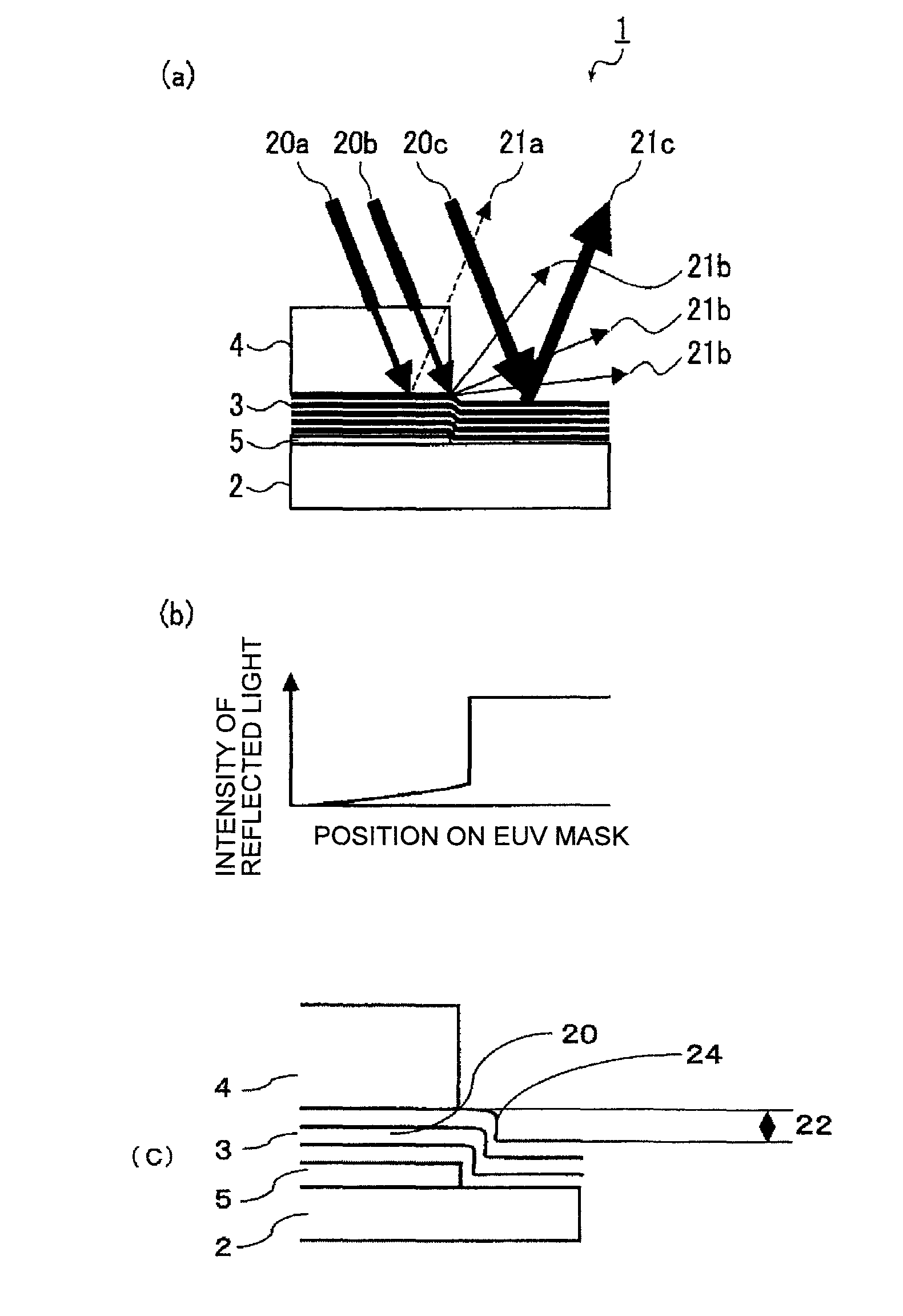
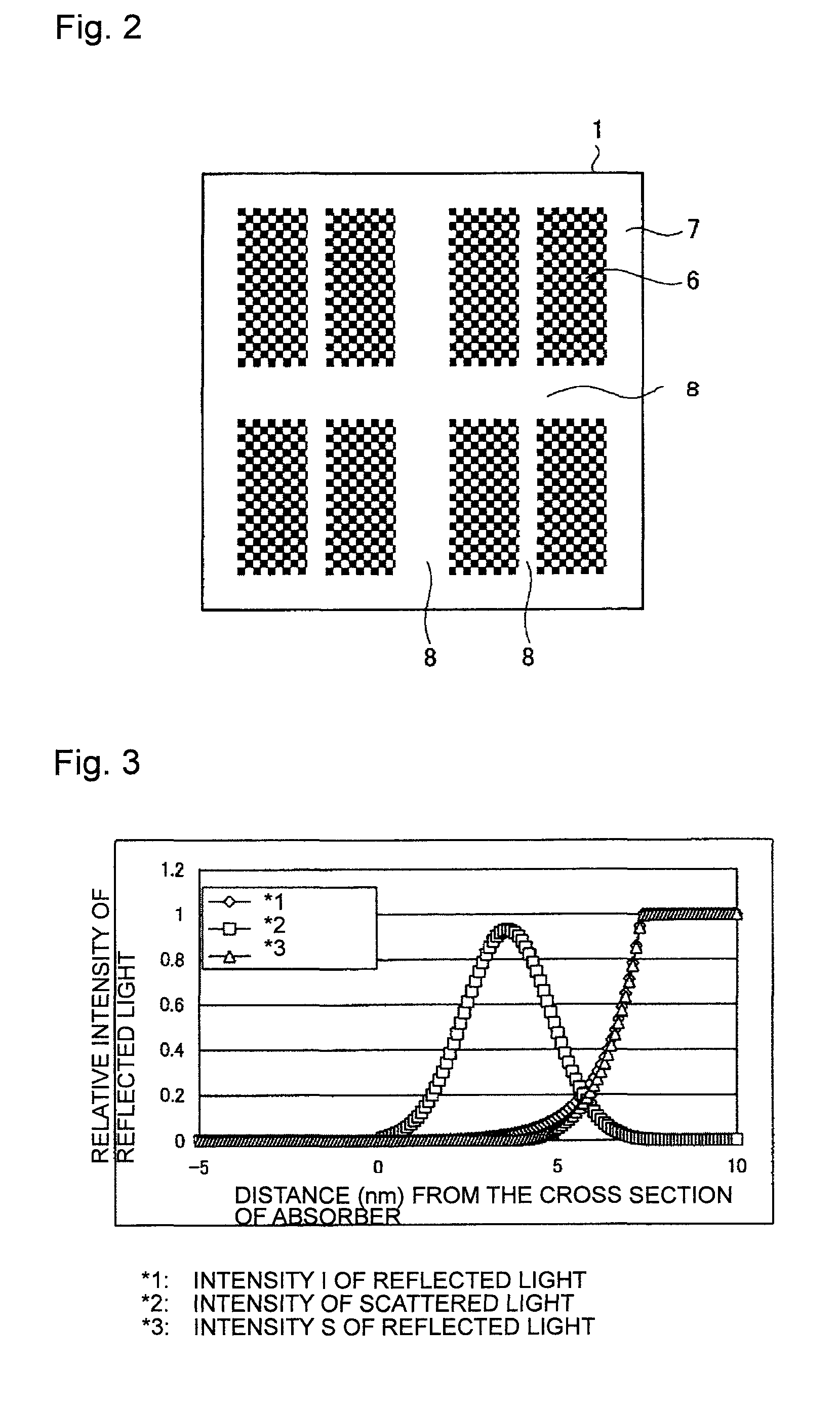
[0133]In Example 1, a simulation assuming a case where an EUV mask having a constitution as shown in FIG. 1(a) is irradiated with EUV light at an incidence angle of 6°, is carried out to obtain a graph illustrating the intensity of reflected light at each portion on the EUV mask as shown in FIG. 1(b). The results are shown in FIG. 3. The results shown in FIG. 3 are obtained by carrying out a simulation under the following conditions.

[0134]Reflective layer 3, absorber layer 4: Assumed reflective layer and absorber layer so that the contrast of reflected light will be 1,000:1

[0135]Thickness of absorber layer: 70 nm

[0136]Height of step: 7 nm

[0137]Distance between the edge of step and mask pattern boundary: 0 nm

[0138]Intensity of scattered light: All around total of intensity of scattered light scattered by the deformed portion present on the reflective layer, assuming a normal distribution curve with a standard deviation of about ⅕ of the distance from the edge of the step to the edge ...

example 2

[0143]In FIG. 2, the same simulation as in Example 1 is carried out under conditions such that the height of the step is 4 nm and the edge of the step 5 in FIG. 1(a) is shifted to the right side in the drawing so that the distance between the edge of the step and the mask pattern boundary is 4 nm. FIG. 4 is a graph illustrating the intensity of reflected light at each portion on an EUV mask obtainable by the simulation.

[0144]As evident from FIG. 4, as a result of providing a step at the mask pattern boundary, in formation of reflected light by the EUV light which has passed through only a part of the absorber layer, the reflected light is scattered by the deformed portion present on the reflective layer, whereby an improvement in the contrast of reflected light at the mask pattern boundary is confirmed. As evident from the comparison between FIGS. 3 and 4, a higher effect of suppressing the contrast of reflected light is obtained in Example 2 than in Example 1.

example 3

[0145]In Example 3, the same simulation as in Example 1 is carried out under conditions such that the reflective layer 3 and the absorber layer 4 are assumed reflective layer and absorber layer so as to achieve a contrast of reflected light of 100:1, the height of the step is 7 nm, and the edge of the step 5 in FIG. 1(a) is shifted to the right side in the drawing so that the distance between the edge of the step and the mask pattern boundary is 1 nm. FIG. 5 is a graph illustrating the intensity of reflected light at each portion of an EUV mask obtainable by the simulation.

[0146]As evident from FIG. 5, as a result of providing a step at the mask pattern boundary, in formation of reflected light by the EUV light which has passed through only a part of the absorber layer, the reflected light is scattered by the deformed portion present on the reflective layer, whereby an improvement in the contrast of reflected light at the mask pattern boundary is confirmed.


PUM

PropertyMeasurementUnit
heightaaaaaaaaaa
wavelengthaaaaaaaaaa

Abstract

To provide an EUV mask of which a decrease in the contrast of reflected light at the mask pattern boundary, particularly a decrease in the contrast of reflected light at the boundary on the mask pattern outer edge, is suppressed, and an EUV mask blank to be used for production of the EUV mask.A reflective mask blank for EUV lithography, comprising:a substrate, and a reflective layer to reflect EUV light, and an absorber layer to absorb EUV light, formed in this order over the substrate,a step on at least a part of the substrate being provided between a first portion where the absorber layer is removed at the time of patterning, and a second portion where the absorber layer is not removed at the time of patterning, adjacent to the first portion where the absorber layer is removed.

Description

TECHNICAL FIELD[0001]The present invention relates to a reflective mask blank (in this specification, hereinafter referred to as “EUV mask blank”) for EUV (Extreme Ultra Violet) lithography to be used for e.g. production of semiconductors, and a reflective mask for EUV lithography (in this specification, hereinafter referred to as “EUV mask”) obtained by patterning the EUV mask blank.BACKGROUND ART[0002]In the semiconductor industry, a photolithography method using visible light or ultraviolet light has been employed as a technique for writing, on a Si substrate or the like, a fine pattern, which is required for forming an integrated circuit comprising such a fine pattern. However, the conventional photolithography method has been close to the resolution limit, while microsizing of semiconductor devices has been accelerated. In the case of the photolithography method, it is said that the resolution limit of a pattern is about ½ of an exposure wavelength, and that even if an immersio...

Claims


Application Information

Patent Timeline
Patent Type & Authority Patents(United States)
IPC IPC(8): G03F1/00G03F1/24
CPCB82Y10/00B82Y40/00G03F1/24H01L21/0275
Inventor KINOSHITA, TAKERU
Owner ASAHI GLASS CO LTD
Why Eureka
Try Eureka