Double data rate memory device having data selection circuit and data paths
a data selection circuit and data path technology, applied in the direction of information storage, static storage, digital storage, etc., can solve the problems of time delay, extensive wire routing in this configuration, and complex structur
- Summary
- Abstract
- Description
- Claims
- Application Information
AI Technical Summary
Benefits of technology
Problems solved by technology
Method used
Image

Examples
Embodiment Construction
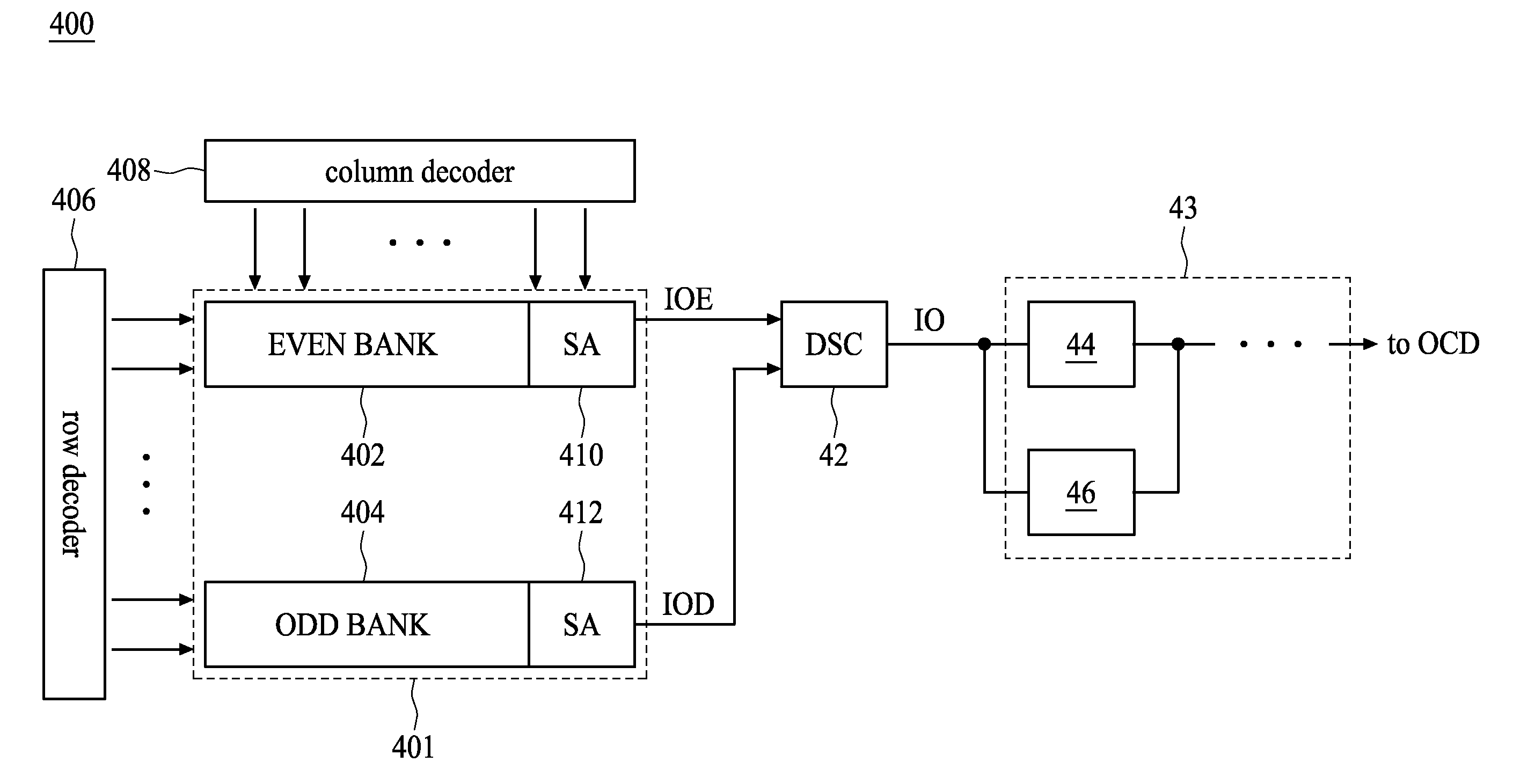
[0023]FIG. 4 shows a block diagram of a double data rate memory device 400 according to one embodiment of the present invention. The memory device 400 comprises a main memory 401 including an even bank 402 and an odd bank 404. Each memory cell of the even and odd banks 402 and 404 is accessed by a row address and a column address decoded by a row decoder 406 and a column decoder 408, respectively, to write data to or read data from the even and odd banks 402 and 404. The read data from the even bank 402 is amplified by a first sense amplifier SA 410, and the amplified data is loaded on an even input and output line IOE. Similarly, the read data from the odd bank 404 is amplified by a second sense amplifier SA 412, and the amplified data is placed on an odd input and output line IOD.
[0024]A data selection circuit DSC 42 is electrically coupled to the even and odd input and output lines IOE and IOD, as shown in FIG. 4. The DSC 42 selects either the even data loaded on the line IOE or ...
PUM
 Abstract
Description
Claims
Application Information
 - R&D
- Intellectual Property
- Life Sciences
- Materials
- Tech Scout
- Unparalleled Data Quality
- Higher Quality Content
- 60% Fewer Hallucinations
Browse by: Latest US Patents, China's latest patents, Technical Efficacy Thesaurus, Application Domain, Technology Topic, Popular Technical Reports.
© 2025 PatSnap. All rights reserved.Legal|Privacy policy|Modern Slavery Act Transparency Statement|Sitemap|About US| Contact US: help@patsnap.com