Method and system for selective stress enablement in simulation modeling

a simulation modeling and stress enablement technology, applied in the direction of instrumentation, design optimisation/simulation, computing, etc., can solve the problem of unacceptably slowing down the design process, and achieve the effect of simulation of the integrated circui

Active Publication Date: 2012-02-07
SIEMENS PROD LIFECYCLE MANAGEMENT SOFTWARE INC
View PDF10 Cites 14 Cited by
  • Summary
  • Abstract
  • Description
  • Claims
  • Application Information

AI Technical Summary

Problems solved by technology

However, adding the effect of such stress to the circuit simulation steps of the integrated circuit design process can be very computer time and resource intensive depending on the restrictions of the methods of implementation, often unacceptably slowing down the design process.

Method used


Image

  • Method and system for selective stress enablement in simulation modeling
  • Method and system for selective stress enablement in simulation modeling
  • Method and system for selective stress enablement in simulation modeling

Examples


Embodiment Construction

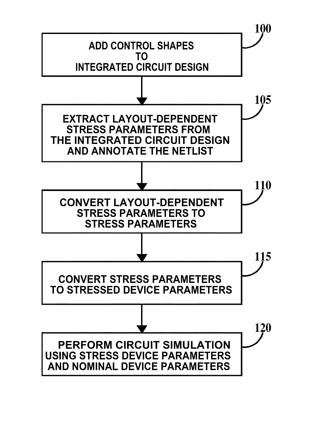
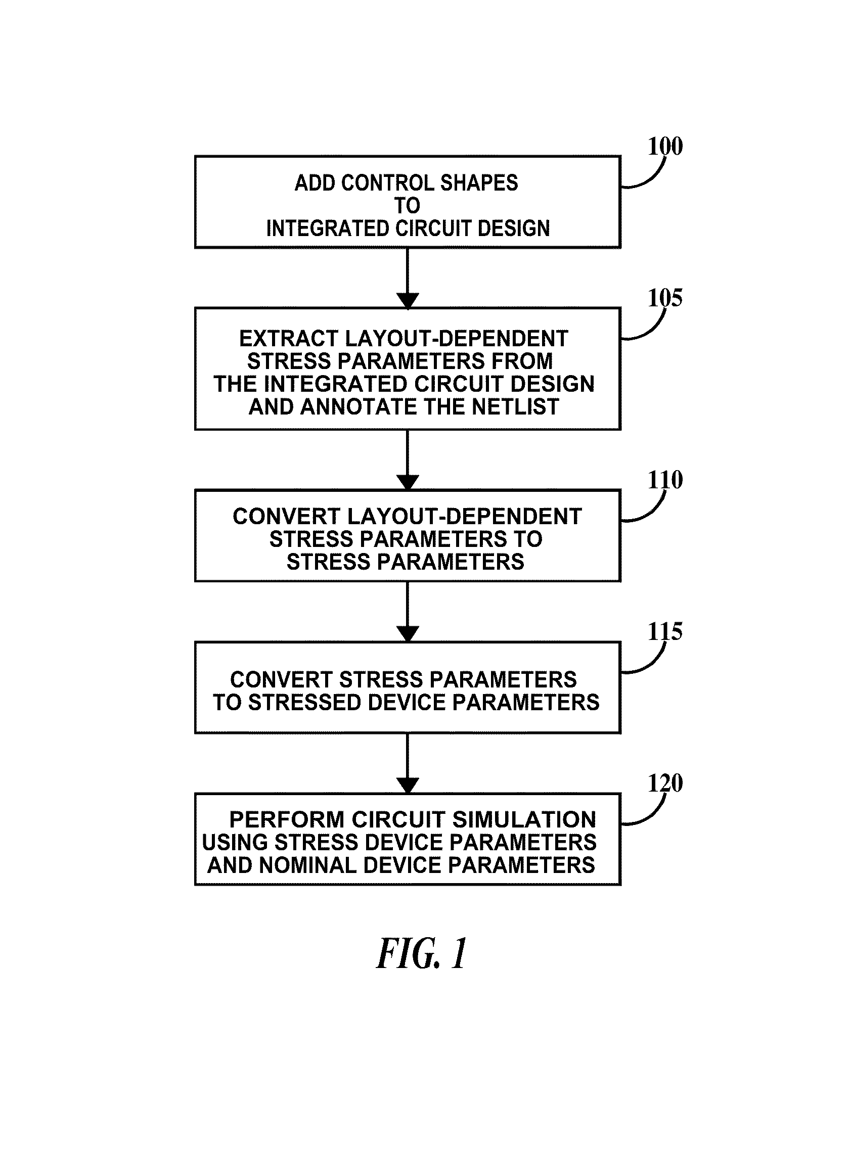
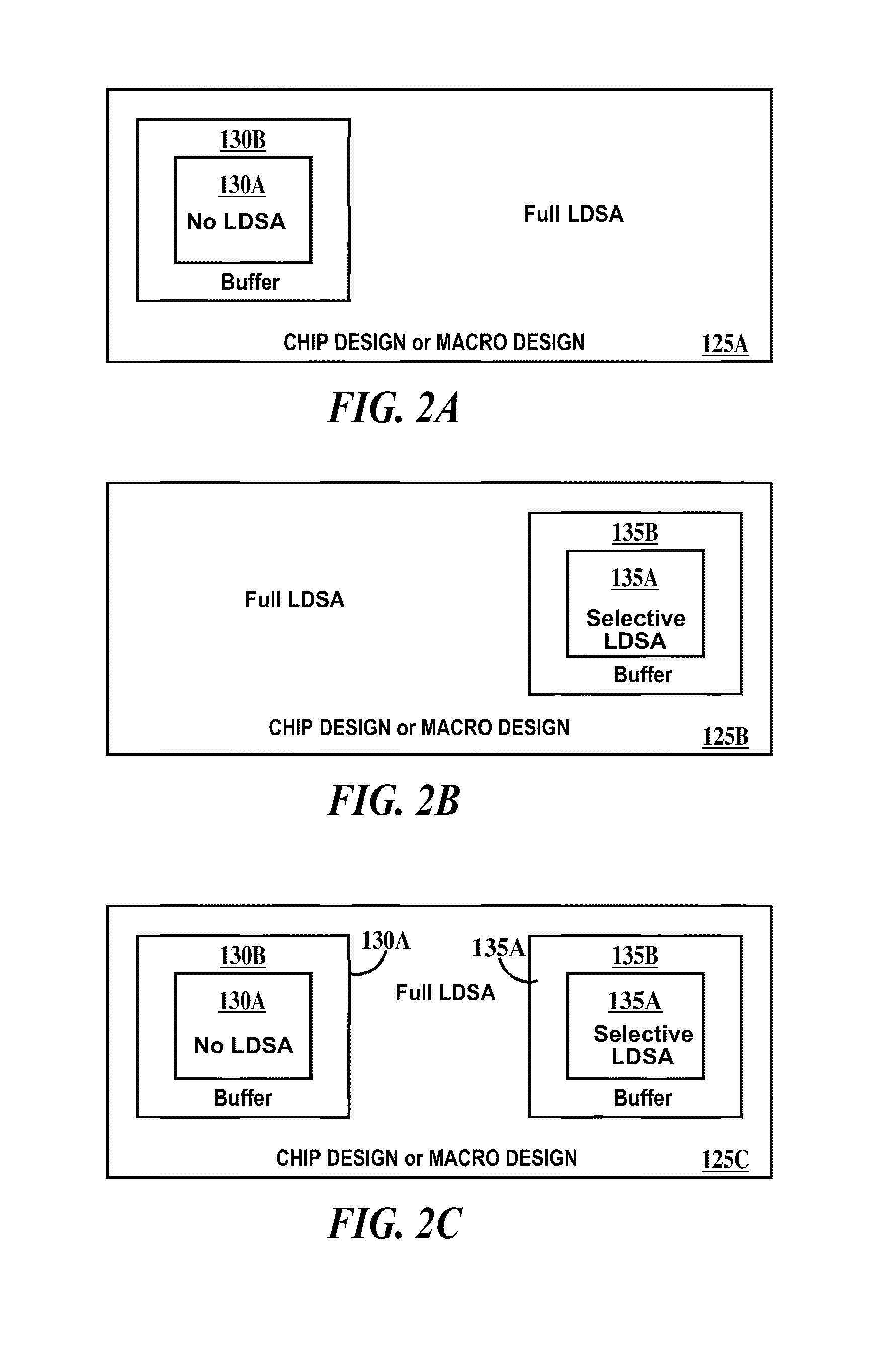
[0014]The embodiments of the present invention reduce the computer time and resource required to determine changes in device parameters due to engineered stress elements when layout changes are made during the design process. Exemplary engineered stress elements include deposited films (e.g., silicon nitride films) with intrinsic tensile or compressive stress that is induced by the deposition process used to form the films. Exemplary engineered stress elements also include heterostructure materials which are materials having heteroatoms such as (e.g., germanium) introduced into the lattice of crystalline materials (e.g., silicon), thereby stressing the material. Heterostructure materials (e.g., silicon germanium) may be used in the source and drain regions of field effect transistors (FETs). Devices include semiconductor (in particular single-crystal semiconductor and more particularly single-crystal silicon) FETs, bipolar transistors, diodes, resistors and capacitors. In particular...


PUM


Abstract

A method and system for modeling an integrated circuit. The method includes converting a representation of the integrated circuit into design shapes of design levels of a design of the integrated circuit; adding control shapes to the design, the control shapes not defining any physical part of the integrated circuit; extracting layout-dependent stress parameters of the devices from the design levels of the design based on the control shapes and the design shapes; converting the layout-dependent stress parameters to stress parameters using a stress algorithm; generating stressed device parameters from the stress parameters using a compact model; and simulating performance of the integrated circuit using the stressed device parameters in a simulation model of the integrated circuit design.

Description

FIELD OF THE INVENTION[0001]The present invention relates to a technique for selective enablement of engineered stress in semiconductor devices for the modeling of integrated circuits.BACKGROUND OF THE INVENTION[0002]Introducing stress into semiconductor devices using engineered stress elements has become an increasing popular method to improve the performance of integrated circuits. However, adding the effect of such stress to the circuit simulation steps of the integrated circuit design process can be very computer time and resource intensive depending on the restrictions of the methods of implementation, often unacceptably slowing down the design process. Accordingly, there exists a need in the art to mitigate the deficiencies and limitations described hereinabove.SUMMARY OF THE INVENTION[0003]A first aspect of the present invention is a method for modeling an integrated circuit having devices, comprising: a method for modeling an integrated circuit having devices, comprising: (a...

Claims


Application Information

Patent Timeline
Patent Type & Authority Patents(United States)
IPC IPC(8): G06F17/50
CPCG06F17/5009G06F30/20
Inventor TONTI, WILLIAM ROBERTWILLIAMS, RICHARD QUIMBY
Owner SIEMENS PROD LIFECYCLE MANAGEMENT SOFTWARE INC
Why Eureka
Try Eureka