Systems and methods for packaging light-emitting diode devices

a technology of light-emitting diodes and packaging methods, applied in semiconductor/solid-state device manufacturing, semiconductor devices, electrical equipment, etc., can solve the problems of increasing package size and manufacturing costs, poor overall efficiency of existing led technologies, and increasing power consumption more than necessary, so as to achieve small package size, higher brightness, and the effect of increasing the brightness

Inactive Publication Date: 2012-02-14
ILLUMITEX INC
View PDF534 Cites 50 Cited by
  • Summary
  • Abstract
  • Description
  • Claims
  • Application Information

AI Technical Summary

Benefits of technology

[0011]For a given flux and emission angle, the size of a packaged LED essentially defines the LED's brightness. Within this disclosure, the term “brightness” may refer to the power of light perceived by the human eye, measurable in units of lumen. For example, if a light source emits one candela of luminous intensity uniformly across a solid angle of one steradian, its total luminous flux emitted into that angle is one lumen. Luminous flux is related to, but differs from radiant flux, the measure of the total power of light emitted. The smaller the package size, the higher the brightness. Brightness is an important characteristic of any light source. The higher the brightness, the easier it is to direct and control the light. For certain applications such as digital light processing (DLP), liquid crystal on silicon (LCOS), spot lights, etc, the light source has to be sufficiently bright to enable the technology. For other applications such as liquid crystal display (LCD) backlights, smaller LED package size translates to thinner, lighter, and more compact display systems.
[0012]In traditionally packaged LED devices such as Luxeon® Rebel and Luxeon® K2 by Philips Lumileds Lighting Company, Cree XLamp® by Cree, Inc., the Dragon® family of high power LEDs by Osram Opto Semiconductors Inc., etc., coupling side emission out of the chip requires the use of reflectors, domes or other secondary optic. This increases the package size as well as the manufacturing costs. With such large packages, the overall system brightness is reduced and thus the overall illumination system efficiency is reduced. Such an efficiency reduction results in more power usage than necessary. Today, most packaged LED chips have side emission and the industry continues to work on how to couple the side emission out of the LED package and make it useable.
[0013]Embodiments disclosed herein can be particularly suitable for packaging LED devices in which the majority of the emitted light comes out of the top of an LED chip and side emission can be negligible. This makes it possible to focus the packaging on directing the emission from the top surface of the LED chip. This also makes it possible for the LED chip to forego domes, reflectors and other secondary optics. Since such an LED chip does not need secondary optics, the LED package can remain similar in dimensions to the LED chip and keep the overall package size very small.
[0017]In some embodiments, the submount and the housing may share an identical or substantially identical foot print. In some embodiments, the submount and the housing may be sized and dimensioned to accommodate a single LED chip. In some embodiments, the submount and the housing may be sized and dimensioned to accommodate an array of LED chips. Examples of an array of LED chips may include, but are not limited to, an array of four LED chips, an array of nine LED chips, an array of sixteen LED chips, an array of twenty-five LED chips, and so on. Because these LED chips do not require domes, reflectors, or other secondary optics, the size of a supporting submount for a LED chip can be minimized, depending on the housing requirement. This allows the overall package size to be very small as compared to traditional packaged LED devices.
[0019]In some embodiments, a method of packaging an LED device may comprise providing a supporting submount and attaching one or more LED chips to the submount. In some embodiments, the Gold-to-Gold Interconnect (GGI) process may be utilized. In some embodiments, solder-based approaches may be used to attach the LED structure or structures to the submount. One advantage of using the GGI process is the high thermal conductivity of gold.
[0021]In some embodiments, the phosphor plate and the housing are joined prior to adhesion to the submount. In some embodiments, the phosphor plate can be positioned within the housing by heat staking. In some embodiments, the phosphor plate can be positioned within the housing using an epoxy that can withstand the high temperature of reflow. In some embodiments, the phosphor plate can be positioned on top of the housing utilizing an adhesive. In some embodiments, the phosphor plate can be made of glass or a clear polymer that can withstand reflow conditions. In some embodiment, phosphor is deposited on top of an LED chip, close to or essentially on the exit face of the LED chip. This is possible because light only comes out the top surface of the LED chip. This unique technological advantage can simplify phosphor deposition and color temperature control.

Problems solved by technology

Existing LED technologies may attempt to increase this ratio, typically referred to as “overall efficiency” or “wall-plug efficiency.” However, existing LED technologies still suffer poor overall efficiency and low extraction efficiency.
This increases the package size as well as the manufacturing costs.
Such an efficiency reduction results in more power usage than necessary.

Method used


Image

  • Systems and methods for packaging light-emitting diode devices
  • Systems and methods for packaging light-emitting diode devices
  • Systems and methods for packaging light-emitting diode devices

Examples


Embodiment Construction

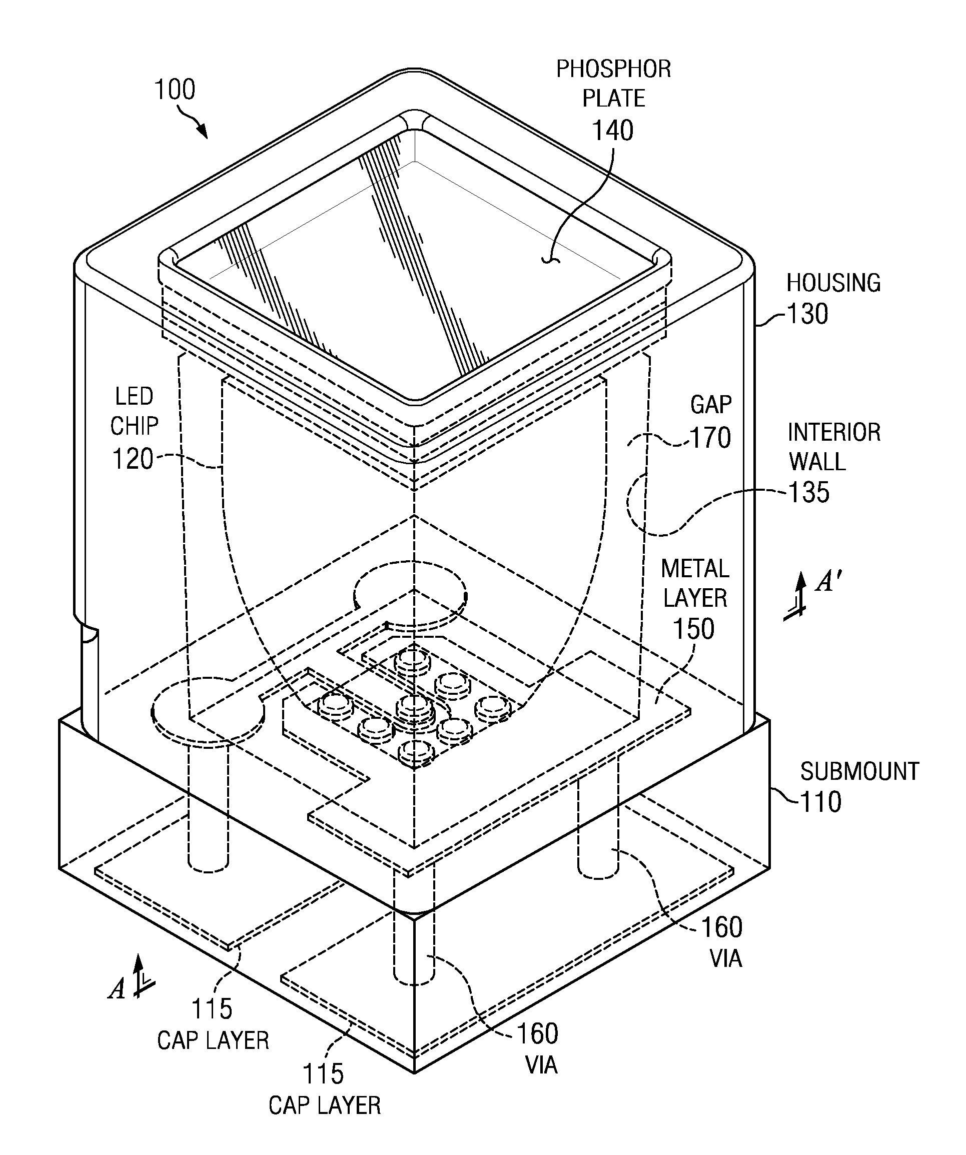
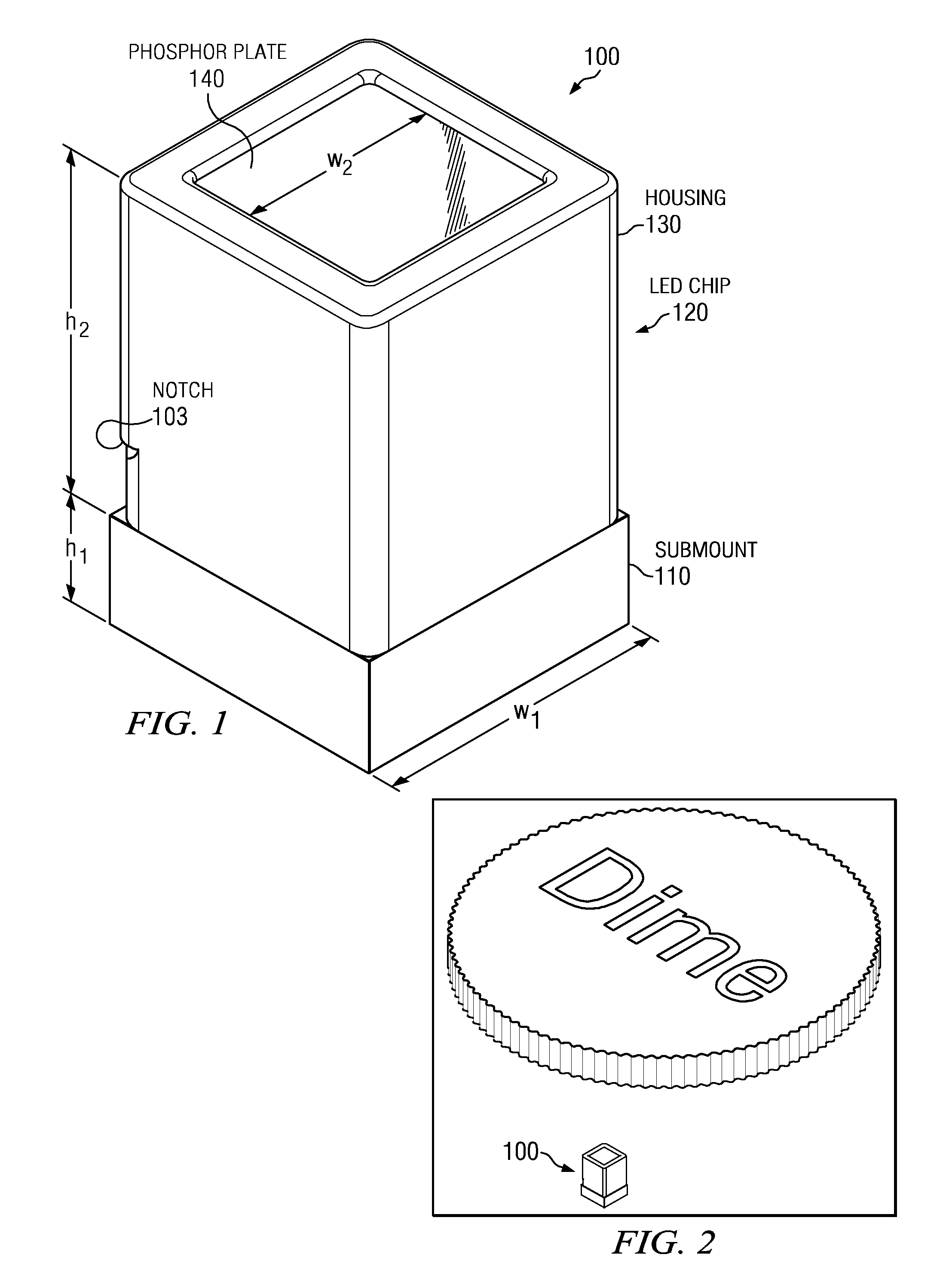
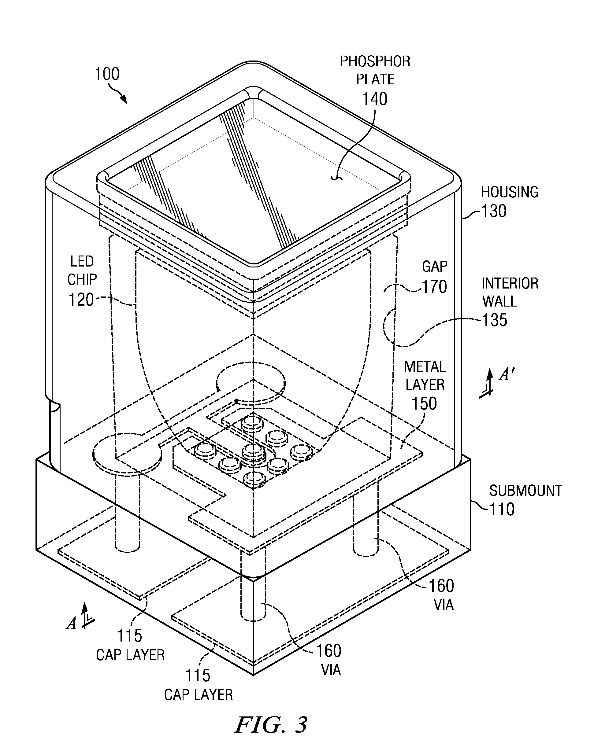
[0035]The disclosure and the various features and advantageous details thereof are explained more fully with reference to the non-limiting embodiments that are illustrated in the accompanying drawings and detailed in the following description. Skilled artisans should understand, however, that the detailed description and the specific examples, while disclosing preferred embodiments, are given by way of illustration only and not by way of limitation. Various substitutions, modifications, additions or rearrangements within the scope of the underlying inventive concept(s) will become apparent to those skilled in the art after reading this disclosure.

[0036]As used herein, the terms “comprises,”“comprising,”“includes,”“including,”“has,”“having” or any other variation thereof, are intended to cover a non-exclusive inclusion. For example, a process, product, article, or apparatus that comprises a list of elements is not necessarily limited only those elements but may include other elements...


PUM


Abstract

Embodiments disclosed herein provide packaged LED devices in which the majority of the emitted light comes out the top of each LED chip with very little side emissions. Because light only comes out from the top, phosphor deposition and color temperature control can be significantly simplified. A package LED may include a housing positioned on a supporting submount, sized and dimensioned to accommodate a single LED chip or an array of LED chips. The LED chip(s) may be attached to the submount utilizing the Gold-to-Gold Interconnect (GGI) process or solder-based approaches. In some embodiments, phosphor may be deposited on top of the LED chip(s) or sandwiched between glass plates on top of the LED chip(s). The phosphor layer may be inside or on top of the housing and be secured to the housing utilizing an adhesive. The housing may be adhered to the submount utilizing a thermal epoxy.

Description

CROSS-REFERENCE TO RELATED APPLICATIONS[0001]This is a conversion of and claims priority from U.S. Provisional Application No. 61 / 121,874, filed Dec. 11, 2008, entitled “SYSTEMS AND METHODS FOR PACKAGING LIGHT-EMITTING DIODE DEVICES” and U.S. Provisional Application No. 61 / 121,870, filed Dec. 11, 2008, entitled “SYSTEMS AND METHODS FOR PACKAGING WHITE LIGHT-EMITTING DIODE DEVICES,” the contents of which are fully incorporated by reference herein for all purposes. The present application also relates to U.S. patent application Ser. No. 11 / 906,194, filed Oct. 1, 2007, entitled “LED SYSTEM AND METHOD” and U.S. patent application Ser. No. 11 / 906,219, filed Oct. 1, 2007, entitled “LED SYSTEM AND METHOD,” both of which are hereby incorporated by reference herein.FIELD OF THE DISCLOSURE[0002]The present disclosure relates generally to light-emitting diode (LED) devices and, more particularly, to systems and methods for packaging LED devices to provide light with the maximum possible overal...

Claims


Application Information

Patent Timeline
Patent Type & Authority Patents(United States)
IPC IPC(8): H01L33/00H01L21/50
CPCH01L33/20H01L33/486H01L33/507H01L33/505H01L2924/0002H01L2924/00
Inventor DUONG, DUNG T.WINBERG, PAUL N.VAZ, OSCAR
Owner ILLUMITEX INC
Why Eureka
Try Eureka