Color image display panel and method of producing the same, and color image display apparatus

a color image and display panel technology, applied in the manufacture of electrode systems, electric discharge tubes/lamps, instruments, etc., can solve the problems of reducing the yield affecting the strength of masks, and affecting the production efficiency of high-definition image display panels. , to achieve the effect of shortening the driving lifetime of devices, reducing the brightness of image display panels, and increasing the current density of devices

Active Publication Date: 2012-02-21
CANON KK
View PDF5 Cites 16 Cited by
  • Summary
  • Abstract
  • Description
  • Claims
  • Application Information

AI Technical Summary

Benefits of technology

[0060]When the value for the slope is neither 1 / 2 nor 1 / 3, the positions of the centers of gravity of the sub-pixels 105 each having a shape of parallelogram do not correspond to the conventional delta array or scramble array of rectangular sub-pixels. However, a two-dimensional, regular color pixel array is established, so a value for a driving current to be applied to each sub-pixel for displaying a predetermined two-dimensional color image can be surely determined, and a desired image can be displayed. When the slope is small, there is no difference between the present invention and a conventional vertical stripe, so the advantage of the present invention, that is, an improvement in resolution upon display of a natural image becomes small.
[0061]On the other hand, when the slope of the sub-pixels each having a shape of parallelogram is large, each sub-pixel narrows, so an occupied area ratio of the sub-pixel to a non-pixel portion reduces, and detrimental effects such as a reduction in brightness of the image display panel, an increase in current density of a device, and the shortening of the driving lifetime of the device cannot be ignored.
[0062]Therefore, a range of the value for the slope of 1 / 5 to 1 / 1 is effective in practical use, though the suitable range of the value is not limited on principle. A value for the slope of 1 / 3 or 1 / 2 is particularly effective because the design of a conventional delta array or scramble array can be utilized.
[0063]Only the sub-pixels 105 having the same luminescent color are arrayed in a linear fashion in the image display panel having the shapes and array of the sub-pixels 105 shown in FIG. 1. In short, the sub-pixels 105 having the same luminescent color are arrayed in a stripe fashion so that the first straight line s connecting the positions of the centers of gravity of the sub-pixels 105 adjacent to each other in the vertical direction is parallel to the two parallel sides of each of the sub-pixels 105. Stripes each obtained by arraying the organic EL devices are arranged so as not to overlap each other and so as to be parallel to each other while being slanted with respect to the vertical line v. As a result, the mask 201 having the stripe-shaped through-holes 202 as schematically exemplified in FIGS. 2A, 2B and 2C can be used in the step of depositing a material for each sub-pixel 105 through a mask onto the substrate.
[0064]FIG. 2A is an explanatory view for a stripe-shaped through-hole portion. Since an interval between the adjacent stripe-shaped through-holes 202 formed in the mask 201 is twice as long as the pitch at which the sub-pixels are arrayed, the shaved portions 203 of the adjacent through-holes can be produced so as not to interfere with each other.
[0065]Although the through-holes 202 may be formed obliquely to the mask 201 as schematically shown in FIG. 2B, the following procedure may be adopted: the through-holes are formed so as to be parallel to each other along the entire shape of the mask 201 as shown in FIG. 2C, and the mask 201 is obliquely rotated in its plane before use. Such processing as shown in FIG. 2C is convenient for an improvement in ease with which a tension is uniformly applied in a stripe direction because the mask 201 is often fixed to a jig before use by applying a predetermined tension. In that case, a second mask having an opening corresponding to the shape of an image display region on the substrate may be overlapped in order that the deposition of a material on a region except the image display region may be prevented.

Problems solved by technology

As a result, the mask involves a problem in terms of strength: the mask is apt to split in a specific direction when an external force is applied to the mask.
In addition, the mask cannot be fixed to a jig by applying a sufficient tension, so the accuracy of position of the vacuum deposition step becomes low, and the yield in which a high-definition image display panel is produced reduces.
In the case of the scramble array, a portion where the shaved portions 203 interfere with each other particularly strongly (not shown) is present, so the resultant mask is apt to tear particularly in an oblique direction, and it becomes additionally difficult to produce a mask that can be put into practical use.
However, the area of each sub-pixel reduces, so the current density of a device must be increased in order that light with predetermined brightness may be emitted, and the increase adversely affects the luminous current efficiency and driving lifetime of an image display panel.
An image display apparatus using the image display panel as a component inherits the problems, so the apparatus involves problems in terms of, for example, cost, performance, and lifetime.
In other words, a conventional color image display panel having rectangular sub-pixels arrayed in a delta array or a scramble array involves the following problem: it is difficult to increase the opening ratio of each sub-pixel when the sub-pixel is produced by a vacuum deposition step involving the use of a mask.
The problem is due to the presence of a portion where the corner portions of sub-pixels are close to each other.
The problem described here is remarkable when a color image display panel is produced by a vacuum deposition step involving the use of a mask having a large opening ratio.

Method used


Image

  • Color image display panel and method of producing the same, and color image display apparatus
  • Color image display panel and method of producing the same, and color image display apparatus
  • Color image display panel and method of producing the same, and color image display apparatus

Examples


example 1

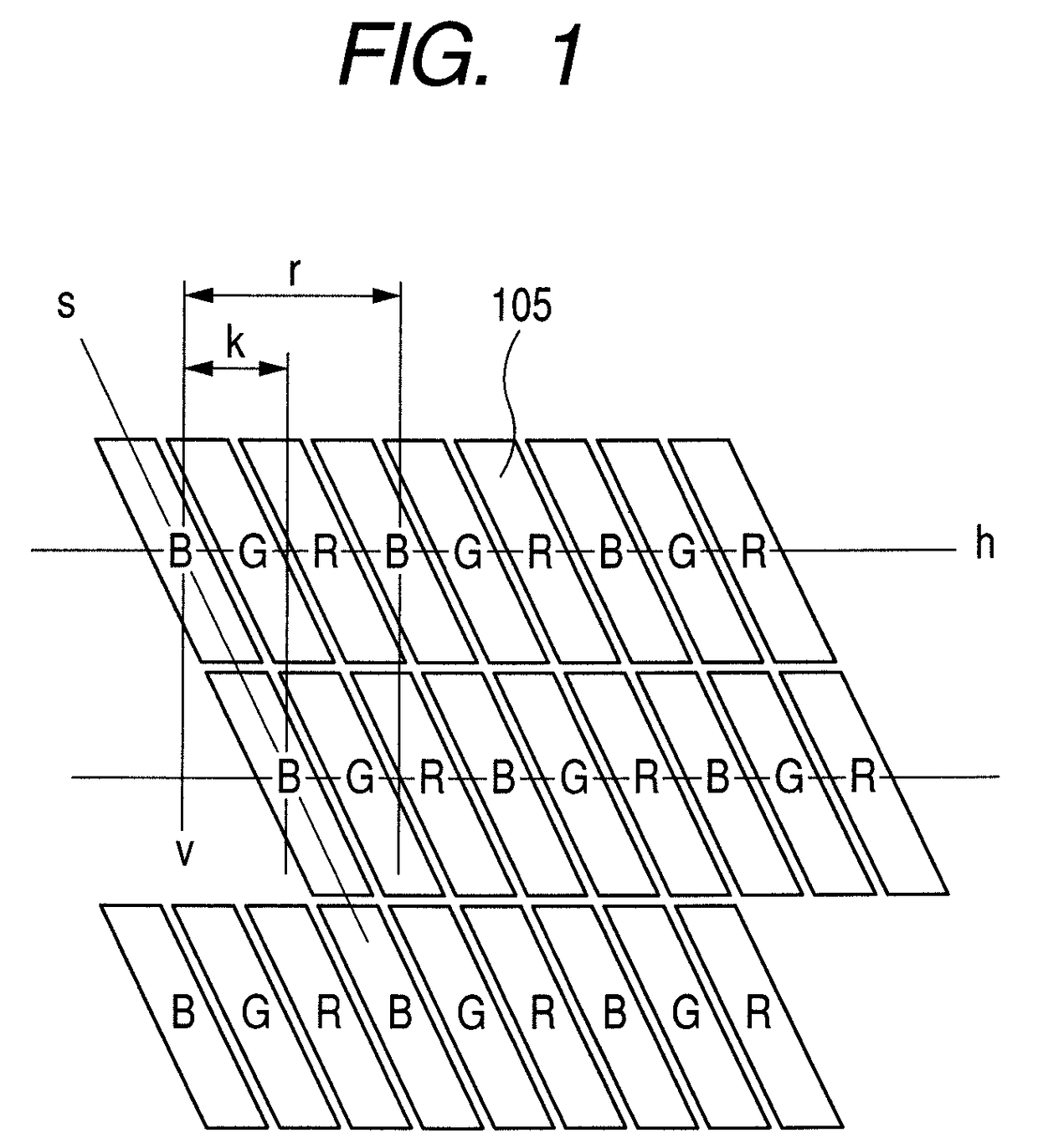
[0141]A method of producing the image display panel of the present invention will be specifically described. A silicon TFT active matrix drive circuit corresponding to 100 ppi is formed on a glass substrate. An insulating / planarizing layer made of an acrylic resin is superimposed on the circuit. A chromium reflecting layer having a thickness of 300 nm and an indium tin oxide layer having a thickness of 0.6 μm each connected to the driver transistor through a through-hole opened in the acrylic resin layer are formed. The chromium reflecting layer and the tin oxide layer are each patterned in the planar shape shown in FIG. 1, whereby a first electrode is obtained. The size of the first electrode, which is of a shape of parallelogram, is as follows: the length of a long side of the parallelogram is 237 μm, and the length of a short side of the parallelogram is 75 μm. An interval between the first electrodes adjacent to each other in a vertical direction is 30 μm, and an interval betwee...

example 2

[0149]Another production example of the image display panel of the present invention will be described.

[0150]An image display portion obtained by arraying 960 columns×240 rows of active matrix drive circuits in accordance with FIG. 9 on a glass substrate, and a silicon TFT substrate on which the latch array 406, and the shift registers 405 and 407 shown in FIG. 10 have been formed are produced. Each of the data signal lines 411 connects a blue sub-pixel in an odd row and a red sub-pixel in an even row, a green sub-pixel in an odd row and a blue sub-pixel in an even row, or a red sub-pixel in an odd row and a green sub-pixel in an even row in the vertical direction. An insulating / planarizing layer made of an acrylic resin is superimposed on the surface of the image display portion. An Ag alloy (AgPdCu) layer having a thickness of 100 nm and connected to each of the driver transistors through a through-hole opened in the acrylic resin layer is deposited. Further, an indium zinc oxide ...

example 3

[0157]A production example of the image display apparatus of the present invention will be described. The display control portion 402 shown in FIG. 10 is connected to the image display panel of Example 2. The controller 409 outputs a V start pulse, and then computes the brightness of each sub-pixel in the first row of the display portion 403 with reference to the video signal conversion memory 408.

[0158]Next, the controller 409 outputs a reset signal for the H shift register. After that, the controller 409 sequentially and serially outputs data on the brightness of each sub-pixel determined by the calculation together with an H shift clock. After the completion of output for one row, the controller 409 outputs a V shift clock to carry out the same treatment as that described above for the next row.

[0159]After the completion of a treatment for the final row, the controller 409 waits for a predetermined time period, and repeats again the same operation commencing on the output of a V ...


PUM


Abstract

There is provided an organic electroluminescence type two-dimensional color image display panel includes multiple arrayed pixels, the pixels being each formed by arranging organic EL devices having at least red, green, and blue luminescent colors in a certain order, in which each of the organic EL devices has a pair of two parallel sides in a planar shape, the organic EL devices having luminescent colors different from each other are adjacent to each other at the two parallel sides, and the organic EL devices having the same luminescent color are adjacent to each other in a parallel line direction of the two parallel sides, and are arrayed to be of shape of stripes arranged parallel to each other while being slanted with respect to a vertical line.

Description

BACKGROUND OF THE INVENTION[0001]1. Field of the Invention[0002]The present invention relates to a color image display panel obtained by arraying multiple organic electroluminescence devices (organic EL devices) each having such a structure that a first electrode, a layer containing at least one kind of a low-molecular-weight luminous organic compound, and a second electrode are laminated in the stated order on a substrate and a method of producing the color image display panel, and a color image display apparatus using the color image display panel.[0003]2. Description of the Related Art[0004]A known organic EL device has such a structure that a first electrode formed on a substrate, an organic compound layer formed on the first electrode, and a second electrode formed on the organic compound layer are laminated.[0005]FIGS. 11A and 11B are each schematic views illustrating an example of an image display panel on which organic EL devices are arrayed in a matrix fashion. FIG. 11A is ...

Claims


Application Information

Patent Timeline
Patent Type & Authority Patents(United States)
IPC IPC(8): H01L27/32H01J9/00
CPCG09G3/3225H01L27/3211C09K2211/1007C09K2211/1011C09K2211/1014G09G2300/0417G09G2300/0443H10K59/35
Inventor YUASA, SATOSHI
Owner CANON KK
Why Eureka
Try Eureka