Magnetic tunnel junction device and fabrication

a technology of magnetic tunnel junction and fabrication, which is applied in the direction of magnetic bodies, instruments, record information storage, etc., can solve the problems of increasing degrading the magnetoresistance (mr), and reducing the current density of high-quality metal/metal-oxide capping layers, etc., to achieve the effect of increasing the switching current density and reducing the switching current density

Active Publication Date: 2012-02-21
QUALCOMM INC
View PDF16 Cites 15 Cited by
  • Summary
  • Abstract
  • Description
  • Claims
  • Application Information

AI Technical Summary

Benefits of technology

[0006]A capping layer adjacent to a free layer of a MTJ device may be formed of a metal layer and layer of a metal oxide. The capping layer including the metal oxide may reduce a switching current density, while the metal layer may prevent diffusion of oxygen from the oxide layer during a magnetic annealing step and, thereby MR reduction. In addition, a high-quality metal / metal-oxide capping layer may not increase RA by enabling coherent tunneling of spin-polarized electrons through the double barrier.
[0009]In another particular embodiment, an apparatus is disclosed that includes means for storing a data value as an orientation of a magnetic moment that is programmable by a spin polarized current exceeding a critical switching current density. The apparatus also includes tunneling barrier means that are thin enough to provide sufficient conduction electrons to the means for storing by quantum mechanical tunneling of conduction electrons through the barrier. The apparatus further includes capping means for reducing a spin pumping effect. The capping means includes a first metal portion and an oxidized metal portion. The means for storing is positioned between the tunneling barrier means and the capping means.

Problems solved by technology

This “spin pumping” effect results in a greater amount of current needed to change a direction of the magnetic moment of the free layer.
However, the additional MgO layer increased the resistance-area product (RA) and degraded the magnetoresistance (MR), which is generally not desirable for securing operating margins for STT-MRAM bitcells.
In addition, a high-quality metal / metal-oxide capping layer may not increase RA by enabling coherent tunneling of spin-polarized electrons through the double barrier.

Method used


Image

  • Magnetic tunnel junction device and fabrication
  • Magnetic tunnel junction device and fabrication
  • Magnetic tunnel junction device and fabrication

Examples


Embodiment Construction

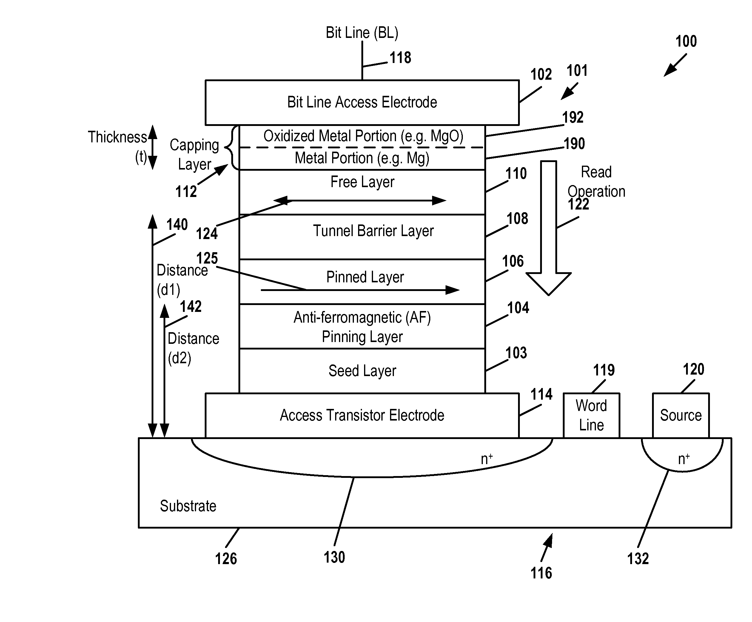
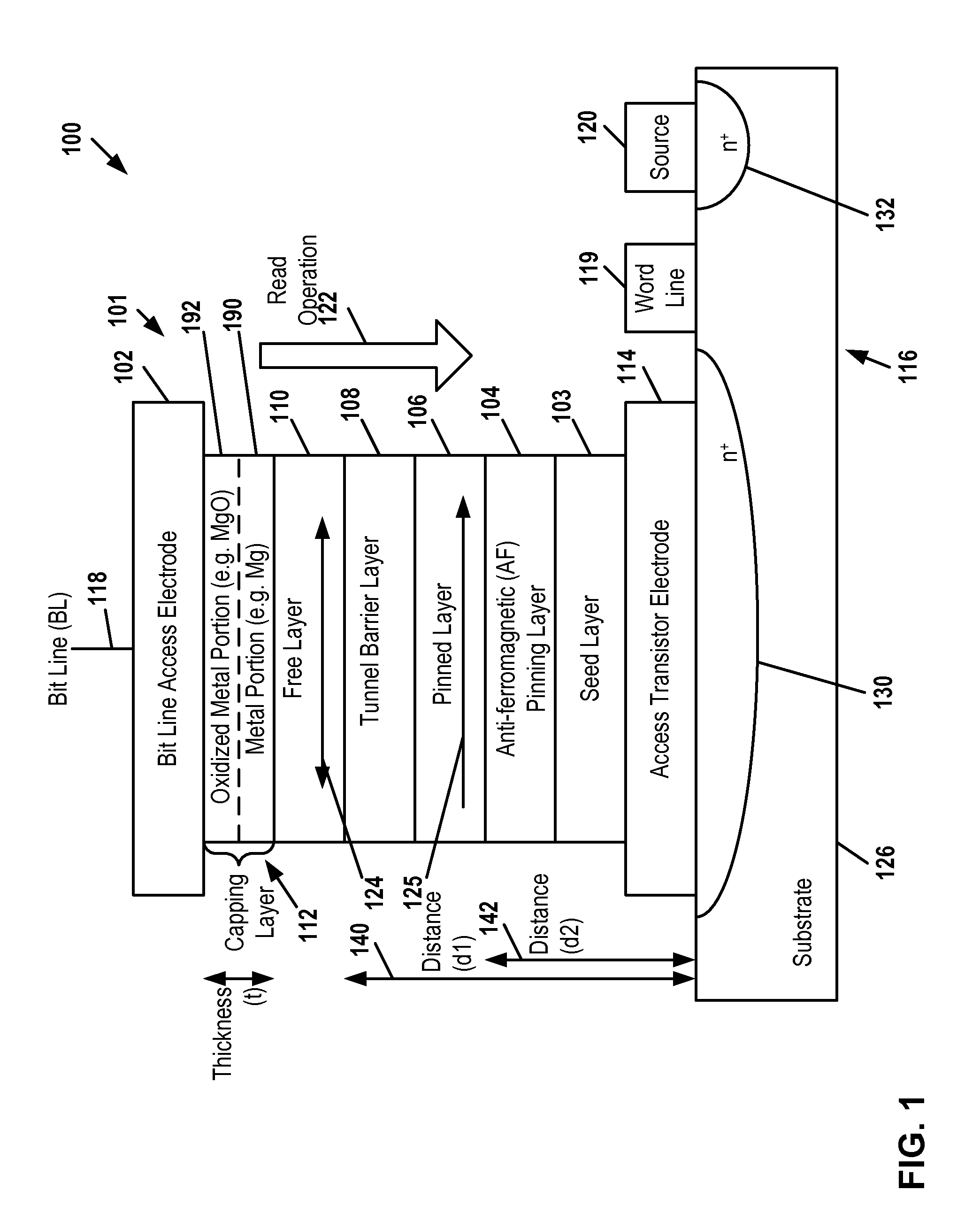
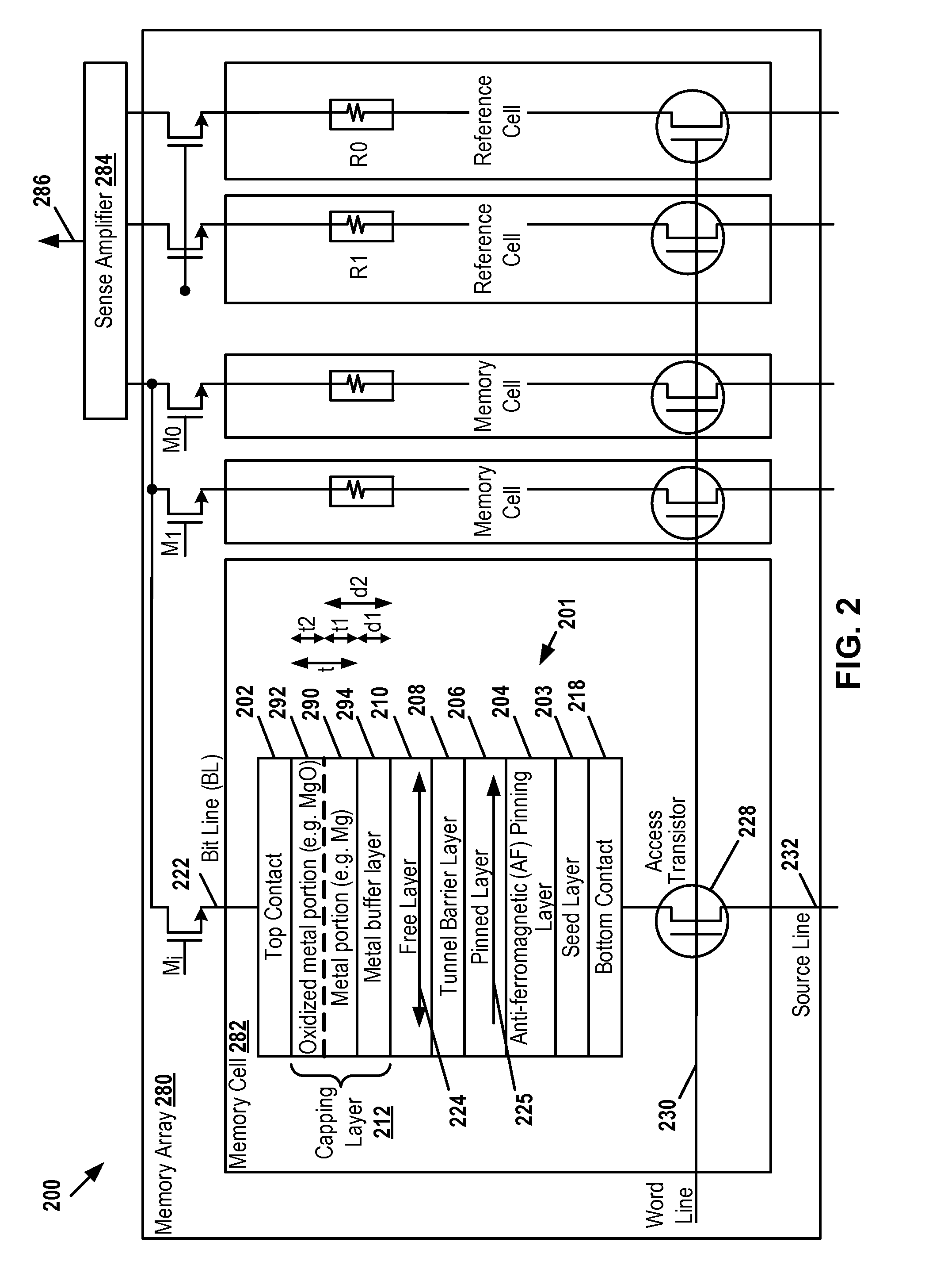
[0018]Referring to FIG. 1, a first illustrative embodiment of an element of a spin-torque-transfer magnetic random access memory (STT-MRAM) is depicted and generally designated 100. The element of the STT-MRAM 100 includes a memory cell having a magnetic tunneling junction (MTJ) device 101 and an access transistor 116 on a substrate 126. The MTJ device 101 includes an access transistor electrode 114, a seed layer 103, an anti-ferromagnetic (AFM) pinning layer 104, a pinned layer 106, a tunnel barrier layer 108, a free layer 110, a capping layer 112, and a bit line access electrode 102 coupled to a bit line 118. The access transistor electrode 114 is coupled to a drain region 130 of the access transistor 116. The access transistor 116 is gated by a word line 119 and has a source region 132 coupled to a source contact 120.

[0019]The seed layer 103 is in contact with the access transistor electrode 114. The seed layer 103 provides a surface for MTJ film deposition and can be composed of...


PUM


Abstract

A magnetic tunneling junction device and fabrication method is disclosed. In a particular embodiment, the method includes depositing a capping material on a free layer of a magnetic tunneling junction structure to form the capping layer and oxidizing a portion of the capping material to form a layer of oxidized material.

Description

I. FIELD[0001]The present disclosure is generally related to magnetic tunneling junction (MTJ) devices and fabrication, and particularly to a MTJ structure that incorporates a capping layer.II. DESCRIPTION OF RELATED ART[0002]MTJ elements may be used to create a magnetic random access memory (MRAM). An MTJ element typically includes a pinned layer, a magnetic tunnel barrier, and a free layer, where a bit value is represented by a magnetic moment in the free layer. A bit value stored by an MTJ element is determined by a direction of the magnetic moment of the free layer relative to a direction of a fixed magnetic moment carried by the pinned layer. The magnetization of the pinned layer is fixed while the magnetization of the free layer may be switched.[0003]When a current flows through the MTJ element, the magnetization direction of the free layer may be changed when the current exceeds a threshold value, i.e. critical switching current (Ic). According to a spin-torque-transfer model...

Claims


Application Information

Patent Timeline
Patent Type & Authority Patents(United States)
IPC IPC(8): H01L29/82G11C11/02
CPCB82Y25/00B82Y40/00G06F17/5068H01F10/3254H01F41/309H01F10/329H01L43/08H01L43/12H01L43/02H01F41/32H01L27/228G06F30/39H10B61/22H10N50/01H10N50/10H01F10/32H10N50/80
Inventor LEE, KANGHOZHU, XIAOCHUNLI, XIAKANG, SEUNG H.
Owner QUALCOMM INC
Why Eureka
Try Eureka