Check patentability & draft patents in minutes with Patsnap Eureka AI!

Single-transistor EEPROM array and operation methods

a technology of eeprom array and single-transistor, which is applied in the field of memory cells, design and operation methods of electrically eraseable programmable readonly memories, can solve the problems of manufacturing process that is not compatible with the formation process of logic mos devices, and the type of eeprom cells suffers from drawbacks, so as to reduce leakage and low operation voltage

Inactive Publication Date: 2012-02-21
TAIWAN SEMICON MFG CO LTD
View PDF10 Cites 0 Cited by
  • Summary
  • Abstract
  • Description
  • Claims
  • Application Information

AI Technical Summary

Benefits of technology

This configuration reduces EEPROM cell size, eliminates the need for selection transistors, and enhances compatibility with logic MOS devices, achieving efficient low-voltage operation and improved resistance to over-erase errors.

Problems solved by technology

This type of EEPROM cell also suffers from drawbacks.
Due to the extra poly, the manufacturing process is not compatible with the formation processes of logic MOS devices, which are single-poly devices.

Method used


Image

  • Single-transistor EEPROM array and operation methods
  • Single-transistor EEPROM array and operation methods
  • Single-transistor EEPROM array and operation methods

Examples


Embodiment Construction

[0016]The making and using of the embodiments of the present invention are discussed in detail below. It should be appreciated, however, that the embodiments provide many applicable inventive concepts that can be embodied in a wide variety of specific contexts. The specific embodiments discussed are merely illustrative of specific ways to make and use the invention, and do not limit the scope of the invention.

[0017]An electrically erasable programmable read-only memory (EEPROM) array is provided. The variations and the operations of the embodiment are then discussed. Throughout the various views and illustrative embodiments of the present invention, like reference numbers are used to designate like elements.

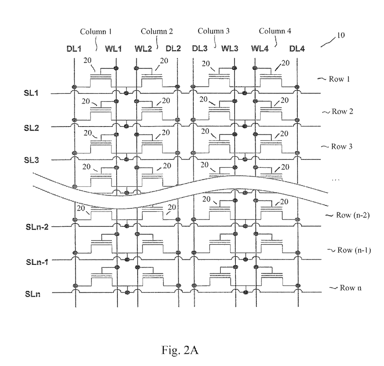
[0018]FIG. 2A illustrates a circuit diagram of EEPROM array 10, which includes a plurality of EEPROM cells 20 arranged in rows (denoted as Row 1, Row 2, and the like) and columns (denoted as Column 1, Column 2, and the like). EEPROM array 10 includes a plurality of word-lines WL ...


PUM


Abstract

An integrated circuit structure includes an electrically erasable programmable read-only memory (EEPROM) array, which includes EEPROM cells arranged as rows and columns; a plurality of word-lines and a plurality of drain-lines extending in a column direction, and a plurality of source-lines extending in a row direction. Each of the plurality of word-lines is connected to control gates of the EEPROM cells in a same column. Each of the plurality of drain-lines is connected to drains of the EEPROM cells in a same column, wherein none of the plurality of drain-lines are shared by neighboring columns of the EEPROM cells. Each of the plurality of source-lines is connected to sources of the EEPROM cells in a same row.

Description

[0001]This application claims the benefit of U.S. Provisional Application No. 61 / 177,545 filed on May 12, 2009, entitled “Single-Transistor EEPROM Array and Operation Methods,” which application is hereby incorporated herein by reference.TECHNICAL FIELD[0002]This invention relates generally to integrated circuit devices, and more particularly to memory cells, and even more particularly to design and operation methods of electrically erasable programmable read-only memories (EEPROMs).BACKGROUND[0003]Electrically erasable programmable read-only memory (EEPROM) has been widely used as the storage device in integrated circuits. There are various types of EEPROMs and corresponding memory cells. FIG. 1 illustrates a portion of a conventional EEPROM array 100, which includes a plurality of memory cells arranged in rows and columns. Word-lines (denoted as CG) and assistance gates AG are parallel to each other and form transistors with the underlying diffusion regions (including the denoted ...

Claims


Application Information

Patent Timeline
Patent Type & Authority Patents(United States)
IPC IPC(8): G11C16/04
CPCG11C16/0416H01L27/11565H01L27/11568G11C16/0433H10B43/30H10B43/10
Inventor WU, CHUN-PEISHIEH, CHIA-TAHUNG, CHIH-WEICHEN, MARS
Owner TAIWAN SEMICON MFG CO LTD
Features
  • R&D
  • Intellectual Property
  • Life Sciences
  • Materials
  • Tech Scout
  • Unparalleled Data Quality
  • Higher Quality Content
  • 60% Fewer Hallucinations
Learn More