White light devices using non-polar or semipolar gallium containing materials and phosphors

a gallium containing material, white light technology, applied in the direction of semiconductor/solid-state device manufacturing, semiconductor devices, electrical devices, etc., can solve the problems of conventional edison light bulbs, conventional light bulbs dissipate much thermal energy, conventional light bulbs routinely fail, etc., to achieve the effect of improving efficiencies and being easy to implemen

Active Publication Date: 2012-02-28
SLT TECH
View PDF135 Cites 185 Cited by
  • Summary
  • Abstract
  • Description
  • Claims
  • Application Information

AI Technical Summary

Benefits of technology

[0017]One or more benefits may be achieved using one or more of the specific embodiments. As an example, the present device and method provides for an improved lighting technique with improved efficiencies. In other embodiments, the present method and resulting structure are easier to implement using conventional technologies. In some embodiments, the present device and method provide a mix of polarized and unpolarized light that are useful in displays and in conjunction with polarizing transmission filters. In a specific embodiment, the blue LED device is capable of emitting electromagnetic radiation at a wavelength range from about 450 nanometers to about 495 nanometers and the yellow-green LED device is capable of emitting electromagnetic radiation at a wavelength range from about 495 nanometers to about 590 nanometers, although there can also be some variations. Depending upon the embodiment, one or more of these benefits can be achieved. These and other benefits are further described throughout the present specification and more particularly below.

Problems solved by technology

Unfortunately, drawbacks exist with the conventional Edison light bulb.
That is, the conventional light bulb dissipates much thermal energy.
Additionally, the conventional light bulb routinely fails often due to thermal expansion and contraction of the filament element.
Unfortunately, achieving high intensity, high-efficiency GaN-based green LEDs has been particularly problematic.
The performance of optoelectronic devices fabricated on conventional c-plane GaN suffer from strong internal polarization fields, which spatially separate the electron and hole wave functions and lead to poor radiative recombination efficiency.
Since this phenomenon becomes more pronounced in InGaN layers with increased indium content for increased wavelength emission, extending the performance of UV or blue GaN-based LEDs to the blue-green or green regime has been difficult.
Furthermore, since increased indium content films often require reduced growth temperature, the crystal quality of the InGaN films is degraded.
The difficulty of achieving a high intensity green LED has lead scientists and engineers to the term “green gap” to describe the unavailability of such green LED.
In addition, the light emission efficiency of typical GaN-based LEDs drops off significantly at higher current densities, as are required for general illumination applications, a phenomenon known as “roll-over.” Other limitations with blue LEDs using c-plane GaN exist.
These limitations include poor yields, low efficiencies, and reliability issues.

Method used


Image

  • White light devices using non-polar or semipolar gallium containing materials and phosphors
  • White light devices using non-polar or semipolar gallium containing materials and phosphors
  • White light devices using non-polar or semipolar gallium containing materials and phosphors

Examples


Embodiment Construction

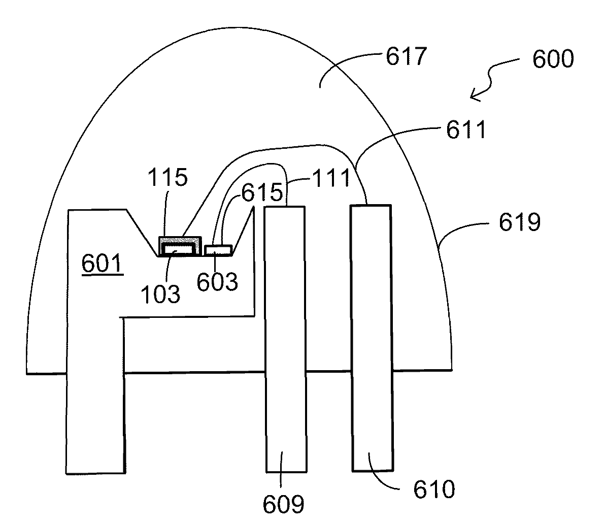
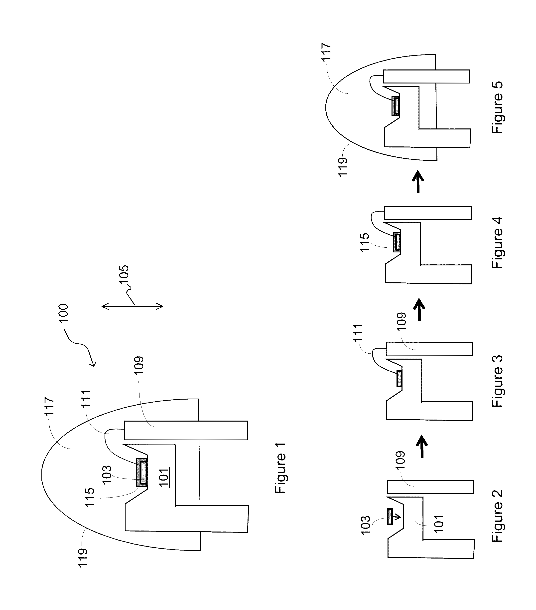
[0030]According to the present invention, techniques generally for lighting are provided. More specifically, embodiments of the invention include techniques for combining one or more colored LED devices, such as violet, blue, blue and yellow, or blue and green, fabricated on bulk semipolar or nonpolar materials with use of entities such as phosphors, which emit light. Merely by way of example, the invention can be applied to applications such as white lighting, multi-colored lighting, general illumination, decorative lighting, automotive and aircraft lamps, street lights, lighting for plant growth, indicator lights, lighting for flat panel displays, other optoelectronic devices, and the like.

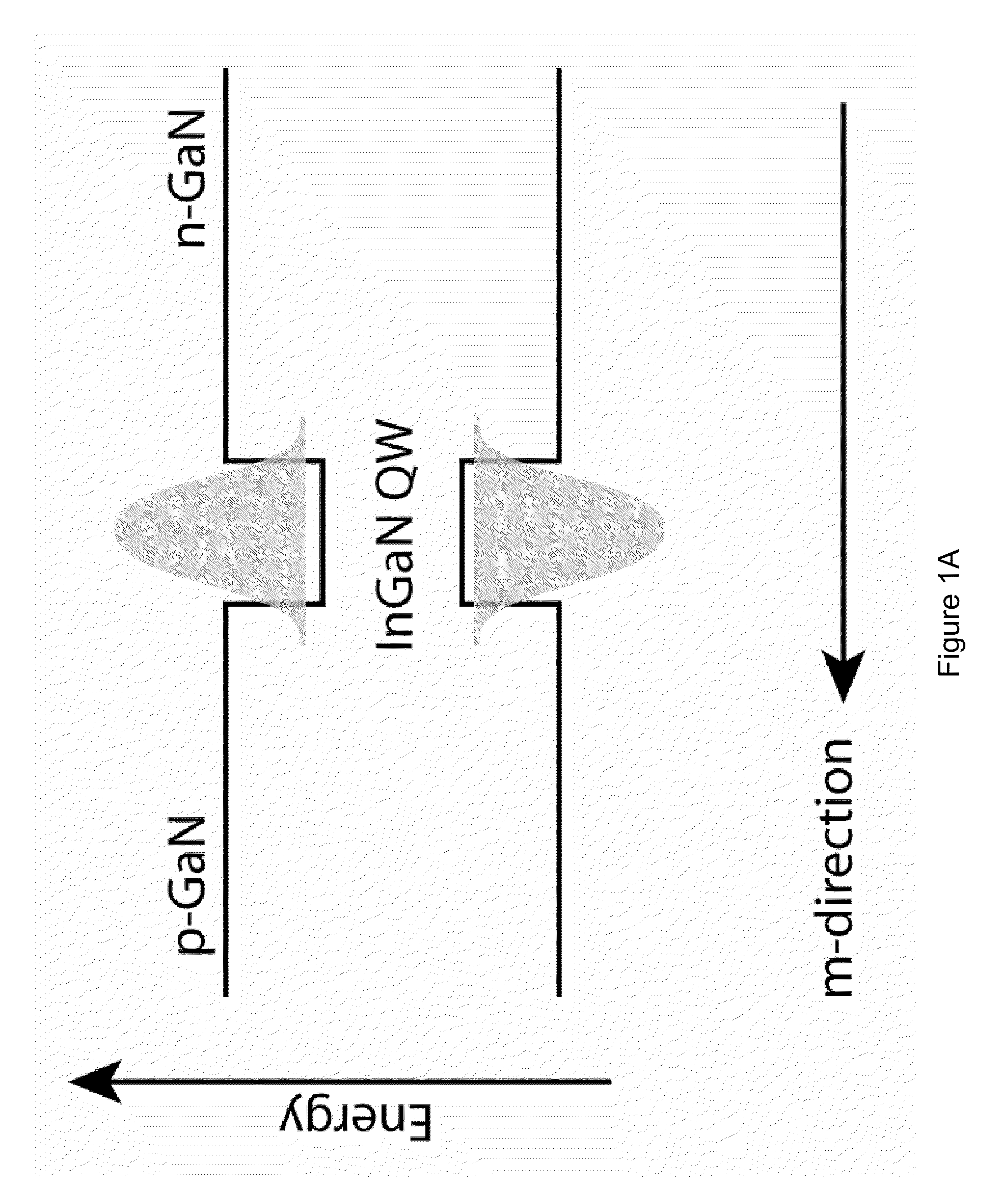
[0031]We have discovered that recent breakthroughs in the field of GaN-based optoelectronics have demonstrated the great potential of devices fabricated on bulk nonpolar and semipolar GaN substrates. The lack of strong polarization induced electric fields that plague conventional devices on c-pl...


PUM


Abstract

A packaged light emitting device. The device includes a substrate member comprising a surface region and one or more light emitting diode devices overlying the surface region. In a specific embodiment, at least one of the light emitting diode device is fabricated on a semipolar or nonpolar GaN containing substrate. The one or more light emitting diode devices are fabricated on the semipolar or nonpolar GaN containing substrate emits substantially polarized emission of one or more first wavelengths. At least at least one of the light emitting diode devices comprise a quantum well region, which is characterized by an electron wave function and a hole wave function. In a specific embodiment, the electron wave function and the hole wave function are substantially overlapped within a predetermined spatial region of the quantum well region. In a specific embodiment, the device has a thickness of one or more entities formed overlying the one or more light emitting diode devices. The one or more entities are excited by the substantially polarized emission and emitting electromagnetic radiation of one or more second wavelengths.

Description

CROSS-REFERENCES TO RELATED APPLICATIONS[0001]This application claims priority to U.S. Provisional Application No. 61 / 086,139, filed on Aug. 4, 2008, commonly assigned, and of which is incorporated by reference in its entirety for all purpose hereby.STATEMENT AS TO RIGHTS TO INVENTIONS MADE UNDER FEDERALLY SPONSORED RESEARCH OR DEVELOPMENT[0002]NOT APPLICABLEREFERENCE TO A “SEQUENCE LISTING,” A TABLE, OR A COMPUTER PROGRAM LISTING APPENDIX SUBMITTED ON A COMPACT DISK[0003]NOT APPLICABLEBACKGROUND OF THE INVENTION[0004]The present invention relates generally to lighting techniques. More specifically, embodiments of the invention include techniques for combining one or more colored LED devices, such as violet, blue, blue and yellow, or blue and green, fabricated on bulk semipolar or nonpolar materials with use of entities such as phosphors, which emit light. Merely by way of example, the invention can be applied to applications such as white lighting, multi-colored lighting, general i...

Claims


Application Information

Patent Timeline
Patent Type & Authority Patents(United States)
IPC IPC(8): H01L33/00
CPCH01L33/32H01L33/502H01L33/16H01L33/54H01L33/58H01L2224/48091H01L2224/48247H01L2224/92247H01L2924/01012H01L2924/0102H01L2924/01025H01L2924/01057H01L2924/01063H01L2924/01078H01L2924/01079H01L2924/09701H01L2224/73265H01L2924/01019H01L2924/01021H01L2924/01037H01L2924/01322H01L2924/00014H01L2924/00H01L2924/12044
Inventor RARING, JAMES W.HALL, ERIC M.D'EVELYN, MARK P.
Owner SLT TECH
Why Eureka
Try Eureka